


AMD Radeon Vega Frontier Edition PCB exposed

AMD Radeon Vega Frontier Edition PCB exposed
 Â
Â
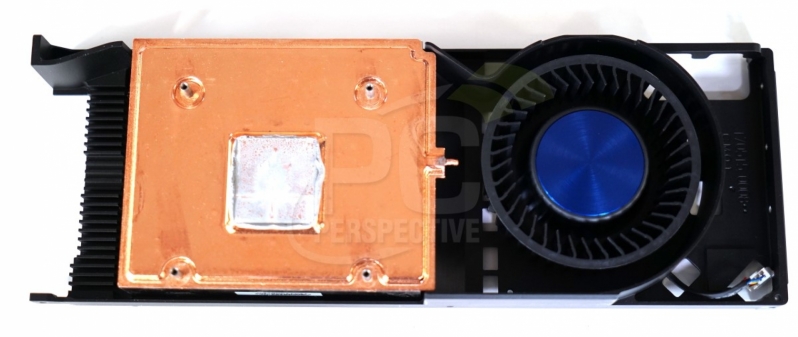
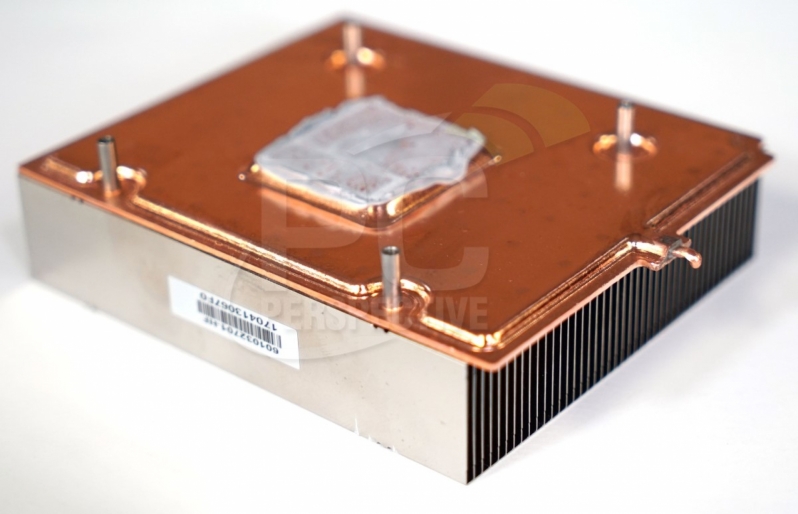
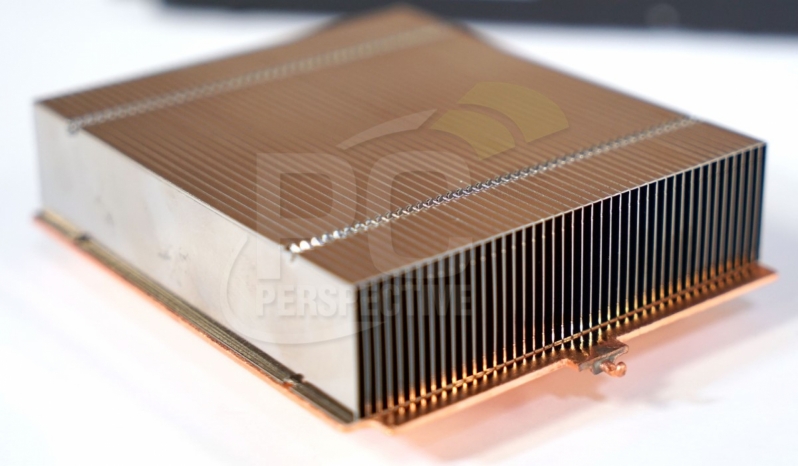
The cooler on this GPU is cooled by a vapour chamber, which then transfers heat onto a copper heat stack that is then cooled by a blower-style fan. The heatsink used here seems a lot smaller than what we see on Nvidia’s GTX Titan series GPUs
It is very interesting to see a similar cooling design as the reference RX 480 on such a high TDP card, though users have not reported R9 290X-style thermals or fan speeds, which means that AMD is certainly not returning back to that era with Vega.Â
Â
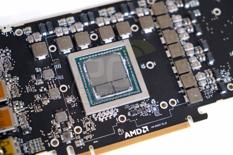
Below we can see the Radeon Vega package, with a GPU die size of 27.85mm x 20.25mm for the GPU excluding the HBM2 memory that is on the same package. This gives a die area of 564mm^2
The whole GPU package is 47.3mm x 47.3mm, giving a package area of 2,237mm^2.Â
Â
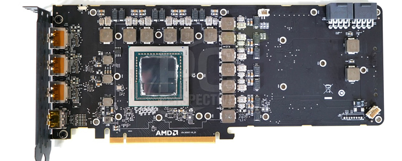
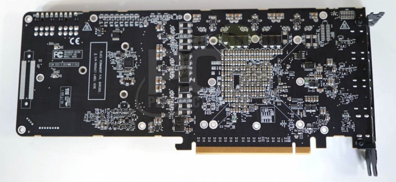
The benefits of AMD’s Radeon Vega design can see seen from the relatively bare PCB, which will allow the company to save on SMT components and on the GPU’s PCB. Even so, the PCB needs to be extended to normal sizes to accommodate a larger cooler design to keep this GPU cool under load.
Â
You can join the discussion on AMD’s Radeon Vega Frontier Edition GPU on the OC3D Forums.
 Â
AMD Radeon Vega Frontier Edition PCB exposed
 Â
Â
The cooler on this GPU is cooled by a vapour chamber, which then transfers heat onto a copper heat stack that is then cooled by a blower-style fan. The heatsink used here seems a lot smaller than what we see on Nvidia’s GTX Titan series GPUs
It is very interesting to see a similar cooling design as the reference RX 480 on such a high TDP card, though users have not reported R9 290X-style thermals or fan speeds, which means that AMD is certainly not returning back to that era with Vega.Â
Â
Below we can see the Radeon Vega package, with a GPU die size of 27.85mm x 20.25mm for the GPU excluding the HBM2 memory that is on the same package. This gives a die area of 564mm^2
The whole GPU package is 47.3mm x 47.3mm, giving a package area of 2,237mm^2.Â
Â
The benefits of AMD’s Radeon Vega design can see seen from the relatively bare PCB, which will allow the company to save on SMT components and on the GPU’s PCB. Even so, the PCB needs to be extended to normal sizes to accommodate a larger cooler design to keep this GPU cool under load.
Â
You can join the discussion on AMD’s Radeon Vega Frontier Edition GPU on the OC3D Forums.
 Â