


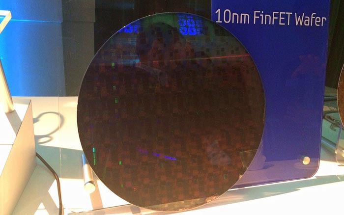
Samsung announces that their 10nm LPP process is now production ready


Samsung announces that their 10nm LPP process is now production ready
Â
With our successful 10LPE production experience, we have commenced production of the 10LPP to maintain our leadership in the advanced-node foundry market, Â
10LPP will be one of our key process offerings for high-performance mobile, computing and network applications, and Samsung will continue to offer the most advanced logic process technology
Â
Â
Just like Samsung’s 14nm FinFETÂ node, it is expected that it will take a while before 10nm will be adopted by large chip makers like AMD, with the process being likely to be used on smaller SoCs and other designs before they can be used on larger chips like desktop grade CPUs and GPUs.Â
Â
You can join the discussion on Samsung’s 10nm process node on the OC3D Forums.Â
Â