


TSMC details their 5nm FinFET process

TSMC details their 5nm FinFET process
5nm will be TSMC’s second process to use EUV (Extreme UltraViolet) lithography, allowing the company to push for some huge increases in transistor density over 7nm, which already offers a 70% area reduction when compared to 16nm. TSMC’s planned 7nm (CLN7FF) node will be the first to make use of EUV technology, though EUV will be used sparingly to reduce complexity, rather than push for significant area reductions.
When compared to 7nm, TSMC’s upcoming 5nm process will not offer much additional performance when compared to a similarly complex chip with the same power draw. TSMC projects that 5nm will deliver a 20% reduction in power consumption with the same performance/complexity or a 15% performance gain with the same power draw and complexity, which is less than half what the projected benefits the move from 16nm to 7nm will achieve. Â
That being said, the clock speeds of chip designs can rely a lot more on chip design than they do on process technologies, with 5nm’s increase in silicon density offering product makers the opportunity to develop silicon with a lot of exciting new features. TSMC has stated that a new “Extremely Low Threshold Voltage” (ELTV) mode will allow chip frequencies to be increased by as much as 25%, though the manufacturer has not gone into great detail about this technology or what kinds of chips it can be applied to.Â
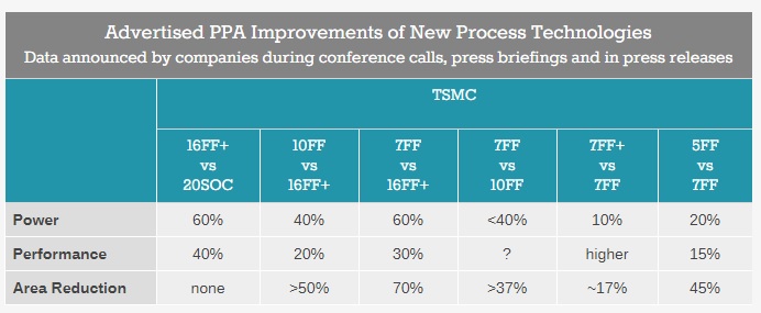
(Table from Anandtech)
 Â
With an Area reduction of 45%, TSMC’s 5nm process will be able to fit 80% more transistors into the same unit of area as 7nm, allowing extremely complex chips to be created using much smaller die sizes.Â
TSMC’s 7nm technology is expected to be ready in 2019, with 5nm coming sometime in 2020, though the main hurdles that will get in the way of production is the current state of EUW technology. Today TSMC uses 145W EUV tools, which is too low to be considered production ready. The company plans to hit 300W with their EUV equipment later this year and use more efficient pellicles to allow more of their EUV light to be usable with their foundry technology. EUV technology is not ready for production today, though it is set to be within the next two years.Â
You can join the discussion on TSMC’s 5nm FinFET manufacturing process on the OC3D Forums.Â