Intel releases information about their 10nm+ Ice lake series of CPUs
Intel releases information about their 10nm+ Ice lake series of CPUs
 Â
These days, most fabs use the ??nm term for marketing, rather than a physical measurement or characteristic of characteristic of their processing node, this has lead to a situation where TSMC is now calling an enhanced version of their 16nm FinFET node 12nm, despite the fact that the size of the node has remained unchanged.  Â
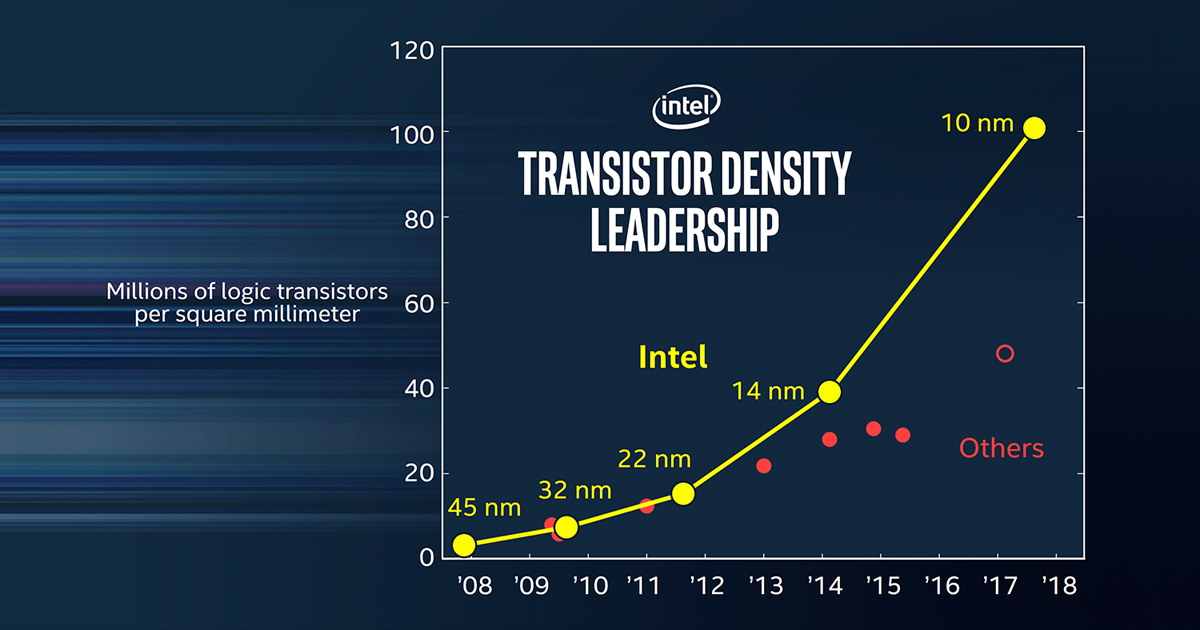
Intel right now is the only major Fab that properly scales their node naming schemes with their process node sizes, giving them what could be defined as the “best” processing technology in terms of transistors per unit area.Â
Â
    The minimum gate pitch of Intel’s 10 nm process shrinks from 70 nm to 54 nm and the minimum metal pitch shrinks from 52 nm to 36 nm. These smaller dimensions enable a logic transistor density of 100.8 mega transistors per mm2, which is 2.7x higher than Intel’s previous 14 nm technology and is expected to be approximately 2x higher than other industry 10 nm technologies.
 Â
With Ice Lake Intel will be moving to their second generation 10nm node, which may make you wonder what happened to 1st generation 10nm, which was not used for any mass produced Intel products.Â
Intel’s 10nm manufacturing process has so far not yielded the performance results that Intel wanted, with their 1st generation node offering either a 25% performance boost over 14nm or 45% lower power draw. Compare this to 14nm++, Intel’s 3rd generation 14nm node, which offers a 26% performance boost or a 26% reduction in power draw when compared to 14nm. Â
This meant that Intel was better off using 14nm++ for now, as 10nm would not yield any performance gains over 14nm++, a node which likely has higher yields and manufacturing capacity. Intel’s baseline 10nm process would be superior for low power designs, but not for high-end products.
Intel has now created their 10nm+ node, which will offer a 15% performance boost over 10nm, with up to a 30% reduction in power, which is more than enough to make it a suitable replacement for 14nm++.Â
Â
Ice Lake is a long way from releasing, but it should be the first full process node advancement from Intel in several generations, which should yield them some noteworthy performance benefits.Â
 Â
You can join the discussion on Intel’s Ice Lake series of CPUs on the OC3D Forums.Â
Â
Special Thanks to TheF34RChannel for providing us with this information.Â


