


ASML passes major EUV milestone

ASML passes major EUV milestone
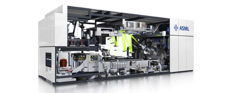
Now the company has created and demonstrated a 250-watt EUV source, with source power being indicative of the number of EUV photons that are exposed to a scanner for wafer exposure and as such is related to the device’s productivity. This source will allow EUV machines to work through 125 WPH (wafers per hour), which many said was the barrier that needed to be passed to make the technology viable for profitable industrial applications. Â
Leading chip makers like Samsung, GlobalFoundries, TSMC and Intel all plan on integrating this technology into their future process nodes, with the extra accuracy provided by EUV allowing for higher resolution lithography. This will, in turn, allow denser more accurate process nodes to be created. With this latest innovation, AMSL’s machines will also be able to work through enough silicon wafers to be profitable, despite the fact that EUV tooling will cost around $100 million each. Â Â
Despite the huge costs of EUV, the technology is expected to prove more economic than today’s triple or quadruple patterning techniques, as EUV will now be able to benefit from faster cycle times and fewer chances of wafer defects.Â
Â
 Â Â
 Â
Â
ASML currently has a backlog of 27 EUV systems, which in total has a value of over 2.8 Billion Euros. A large number of these machines have been purchased by Intel, to help maintain their process node leadership.Â
Back in 2012, the company was only able to create EUV technology that offered a mere 25W source power, marking a 10X increase over the past five years. Now EUV is set to become relevant within silicon manufacturing, with AMSL expecting a further €2.2 Billion in sales next quarter.
Â
You can join the discussion on AMSL’s EUV achievements on the OC3D Forums.Â
Â
ASML passes major EUV milestone
Now the company has created and demonstrated a 250-watt EUV source, with source power being indicative of the number of EUV photons that are exposed to a scanner for wafer exposure and as such is related to the device’s productivity. This source will allow EUV machines to work through 125 WPH (wafers per hour), which many said was the barrier that needed to be passed to make the technology viable for profitable industrial applications. Â
Leading chip makers like Samsung, GlobalFoundries, TSMC and Intel all plan on integrating this technology into their future process nodes, with the extra accuracy provided by EUV allowing for higher resolution lithography. This will, in turn, allow denser more accurate process nodes to be created. With this latest innovation, AMSL’s machines will also be able to work through enough silicon wafers to be profitable, despite the fact that EUV tooling will cost around $100 million each. Â Â
Despite the huge costs of EUV, the technology is expected to prove more economic than today’s triple or quadruple patterning techniques, as EUV will now be able to benefit from faster cycle times and fewer chances of wafer defects.Â
Â
 Â
Â
ASML currently has a backlog of 27 EUV systems, which in total has a value of over 2.8 Billion Euros. A large number of these machines have been purchased by Intel, to help maintain their process node leadership.Â
Back in 2012, the company was only able to create EUV technology that offered a mere 25W source power, marking a 10X increase over the past five years. Now EUV is set to become relevant within silicon manufacturing, with AMSL expecting a further €2.2 Billion in sales next quarter.
Â
You can join the discussion on AMSL’s EUV achievements on the OC3D Forums.Â
Â