


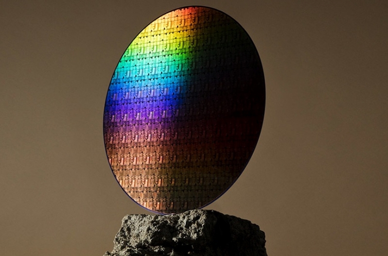
IBM and Samsung reveals “Breakthrough” Transistors that promise boosted performance and efficiency


IBM and Samsung’s VTFET could transform future electronics
Transistor design is a vital part of modern electronics, acting as a driver behind the performance and power efficiency of modern electronics. There is more to transistor design than simply making transistors smaller, their design matters, and IBM and Samsung believe that their latest transistor designs have the ability to transform future semiconductor devices.Â
So what has Samsung and IBM created? They have created Vertical Transport Field Effect Transistors, VTFET transistors. These transistors innovate by “utilizing a new vertical transistor architecture that demonstrates a path to scaling beyond nanosheet”. When compared to equivalently sized FinFET transistors, VTFET transistors can reduce energy use by 85% while offering equivalent or deliver an approximate 2x performance boost with the same power draw. For mobile phones, these transistors could enable the creation of devices that have a week-long battery life, or future chips that can push computational performance to new heights.Â
With these new vertical transistors, Samsung and IBM have also created a pathway towards device scaling “beyond nanosheet”, with nanosheet being the transistor technology that is due to replace FinFETs with future lithography nodes. In this sense, VTFETs are being positioned by IBM and Samsung as a next-next-generation technology.
Technologies like VTFET are painting a bright future for the semiconductor industry, putting to bed claims that there will soon be little room for innovation with future semiconductor/transistor technologies. IBM and Samsung are proving that there is plenty of room for improvement with regards to transistor design, and it likely won’t be long before we see their competitors reveal their own post nanosheet/GAAFET/RibbonFET transistor designs.Â
What follows is IBM’s press release regarding their new VTFET transistor technology.Â
PR – IBM and Samsung Unveil Semiconductor Breakthrough That Defies Conventional Design
Today, IBM and Samsung Electronics jointly announced a breakthrough in semiconductor design utilizing a new vertical transistor architecture that demonstrates a path to scaling beyond nanosheet, and has the potential to reduce energy usage by 85 percent compared to a scaled fin field-effect transistor (finFET)1. The global semiconductor shortage has highlighted the critical role of investment in chip research and development and the importance of chips in everything from computing, to appliances, to communication devices, transportation systems, and critical infrastructure.
The two companies’ semiconductor innovation was produced at the Albany Nanotech Complex in Albany, NY, where research scientists work in close collaboration with public and private sector partners to push the boundaries of logic scaling and semiconductor capabilities. This collaborative approach to innovation makes the Albany Nanotech Complex a world-leading ecosystem for semiconductor research and creates a strong innovation pipeline, helping to address manufacturing demands and accelerate the growth of the global chip industry.
The new vertical transistor breakthrough could help the semiconductor industry continue its relentless journey to deliver significant improvements, including:
– Potential device architecture that enables semiconductor device scaling to continue beyond nanosheet.
– Cell phone batteries that could go over a week without being charged, instead of days.
– Energy intensive processes, such as cryptomining operations and data encryption, could require significantly less energy and have a smaller carbon footprint.
– Continued expansion of Internet of Things (IoT) and edge devices with lower energy needs, allowing them to operate in more diverse environments like ocean buoys, autonomous vehicles, and spacecraft.
   Today’s technology announcement is about challenging convention and rethinking how we continue to advance society and deliver new innovations that improve life, business and reduce our environmental impact,” Dr. Mukesh Khare, Vice President, Hybrid Cloud and Systems, IBM Research. “Given the constraints the industry is currently facing along multiple fronts, IBM and Samsung are demonstrating our commitment to joint innovation in semiconductor design and a shared pursuit of what we call ‘hard tech.’
Moore’s Law, the principle that the number of transistors incorporated in a densely populated IC chip will approximately double every two years, is quickly nearing what are considered insurmountable barriers. Simply put, as more and more transistors are crammed into a finite area, engineers are running out of space.
Historically, transistors have been built to lie flat upon the surface of a semiconductor, with the electric current flowing laterally, or side-to-side, through them. With new Vertical Transport Field Effect Transistors, or VTFET, IBM and Samsung have successfully implemented transistors that are built perpendicular to the surface of the chip with a vertical, or up-and-down, current flow.
The VTFET process addresses many barriers to performance and limitations to extend Moore’s Law as chip designers attempt to pack more transistors into a fixed space. It also influences the contact points for the transistors, allowing for greater current flow with less wasted energy. Overall, the new design aims to deliver a two times improvement in performance or an 85 percent reduction in energy use as compared to scaled finFET alternatives.
Recently, IBM announced the 2 nm chip technology breakthrough which will allow a chip to fit up to 50 billion transistors in a space the size of a fingernail. VTFET innovation focuses on a whole new dimension, which offers a pathway to the continuation of Moore’s Law.
Innovation at the Albany Nanotech Complex is often directed towards commercialization, and on that end of the chip lifecycle today the companies also announced that Samsung will manufacture IBM’s chips at the 5 nm node. These chips are anticipated to be used in IBM’s own server platforms. This follows the announcement in 2018 that Samsung would manufacture IBM’s 7 nm chips, which became available in the IBM Power10 family of servers earlier this year. The IBM Telum processor, also revealed earlier this year, is similarly manufactured by Samsung using IBM’s designs.
IBM’s legacy of semiconductor breakthroughs also includes the first implementation of 7 nm and 5 nm process technologies, High-k metal gate technology, channel SiGe transistors, single cell DRAM, the Dennard Scaling Laws, chemically amplified photoresists, copper interconnect wiring, Silicon on Insulator technology, multi core microprocessors, embedded DRAM, and 3D chip stacking.
1 – VTFET nanosheet and scaled FinFET device simulation results are compared at the same footprint and at an aggressive sub-45nm gate pitch. VTFET nanosheets provides ~ 2X performance of the scaled FinFET at equivalent power due to VTFET maintaining good electrostatics and parasitics while FinFET performance is impacted by severe scaling constraints. Or VTFET could provide as much as 85% power reduction compared to the scaled FinFET architecture as compared at an equivalent frequency on the extrapolated power-performance curves.
You can join the discussion on IBM and Samsung’s VTFET technology on the OC3D Forums.