


Samsung has created its first 3nm GAAFET prototypes – Transistors beyond FinFET


Samsung has created its first 3nm GAAFET prototypes – Transistors beyond FinFET
To meet this target, Samsung is investing in several new technologies, moving beyond the FinFET structure of most modern transistors towards a new design called GAAFET. This week, Samsung has reportedly confirmed that it has produced its first prototypes using its planned 3nm GAAFET node, a major step towards its eventual mass production.Â
When compared to Samsung’s upcoming 5nm node, 3nm GAAFET is designed to deliver increased performance levels, improved density and considerable reductions in power consumption. Samsung estimates that its 3nm GAAFET node will offer a 35% increase in silicon density and a 50% reduction in power consumption or a 35% increase in performance over 5nm.Â
Samsung, when it initially announced its 3nm GAAFET node, reported that it planned to start mass production in 2021, which is an ambitious target for such an advanced node. If successful, Samsung has an opportunity to take market share from TSMC, assuming that Samsung’s technology can provide better performance or density than TSMC’s offerings.Â
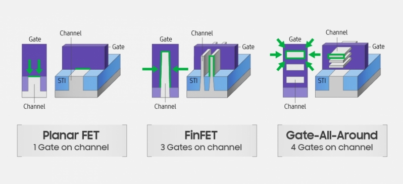
What’s special about GAAFET
Samsung’s GAAFET is an evolution of the FinFET structure that’s used in most of today’s high-end process technologies, providing users with a four-gate structure around the transistor’s channels. This is what gives GAAFET its Gate-All-Around name, as the design’s 4-gate architecture covers all sides of the channel and reduces power leakage.Â
To simplify things, surrounding the channel with gates reduces power leakage, which in-turn allows Samsung to control the channels of their transistors better. Lowering power leakage also allows a higher percentage of a transistor’s power to be used, increasing power efficiency and performance. Reducing power leakage can also help Samsung miniaturise its process tech. In short, Samsung is betting on GAAFET to push its technology ahead of TSMC.Â
If 3nm proves successful, Samsung will gain significant power consumption and performance benefits, which will prove useful as the company searches for new customers. Â
 Â
You can join the discussion on Samsung producing its first 3nm GAAFET chips on the OC3D Forums.Â