
Globalfoundries readies their 7nm process
Globalfoundries has now opened up their 7nm LP (Leading Performance) process up to partners for product designs, a move which will likely attract industry giants like AMD for the creation of their next generation Zen 2 and Navi CPU and GPU products.
This new node hosts some impressive characteristics, with GlobalFoundries touting up to a 40% increase in device performance or a 60% power reduction when compared to 14nm, making 7nm LP attractive to both high-power device makers like AMD as well as the relatively low-power SoC market.
Globalfoundries also states that this new node is EUV compatible but can also use traditional optical lithography, depending on the exact needs of the user. Globalfoundries also states that this new node will also bring in a 30% reduction in die costs, with up to 45% reductions in certain “target segments”.
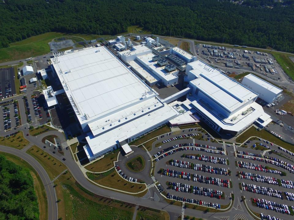
(Globalfoundries FAB 8, Saratoga County New York, where 7nm products will be manufactured)
7nm LP looks like it will be a very attractive offering from Globalfoundries, with the node commercialising in 2018, which isn’t that far away from a marketing standpoint. This process will likely regain the company some business in the low-power SoC market, especially from TSMC who are their main competitors.
You can join the discussion on Globalfoundries new 7nm LP manufacturing process on the OC3D Forums.
Globalfoundries readies their 7nm process
Globalfoundries has now opened up their 7nm LP (Leading Performance) process up to partners for product designs, a move which will likely attract industry giants like AMD for the creation of their next generation Zen 2 and Navi CPU and GPU products.
This new node hosts some impressive characteristics, with GlobalFoundries touting up to a 40% increase in device performance or a 60% power reduction when compared to 14nm, making 7nm LP attractive to both high-power device makers like AMD as well as the relatively low-power SoC market.
Globalfoundries also states that this new node is EUV compatible but can also use traditional optical lithography, depending on the exact needs of the user. Globalfoundries also states that this new node will also bring in a 30% reduction in die costs, with up to 45% reductions in certain “target segments”.
(Globalfoundries FAB 8, Saratoga County New York, where 7nm products will be manufactured)
7nm LP looks like it will be a very attractive offering from Globalfoundries, with the node commercialising in 2018, which isn’t that far away from a marketing standpoint. This process will likely regain the company some business in the low-power SoC market, especially from TSMC who are their main competitors.
You can join the discussion on Globalfoundries new 7nm LP manufacturing process on the OC3D Forums.