Intel confirms steady 18A yield improvements and 14A progress

Intel expects its margins to improve thanks to consistent 18A yield increases
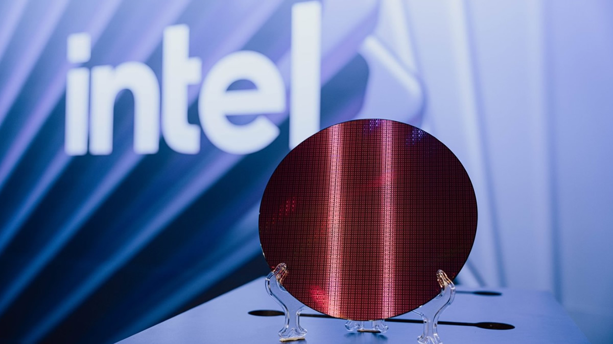
In early 2026, Intel plans to release its 18A Panther Lake series CPUs. This means that Intel’s newest CPUs will be built using Intel silicon, not TSMC silicon. With this change, Intel will increase its margins and utilise its foundry technology. Now, Intel has confirmed that its 18A yield is improving.
Intel’s John Pitzer has stated that Intel’s 18A yields have improved significantly over the past 7-8 months. Now, average yield improvements are around 7% per month, steadily increasing the company’s manufacturing efficiency. Intel is now scaling production of its 18A Panther Lake CPUs for mass production. With higher yields, Intel will have more usable CPUs per silicon wafer, reducing its per-unit manufacturing costs.
Strong yields are vital for Intel’s success as a foundry. After all, Intel’s processors need to be both performant and cost-effective. Throughout 2026, Intel expects its 18A yields to continue to improve. This will increase Intel’s profitability.
We clearly want to do better on the gross margin side. I think what’s important is when Lip-Bu joined in March, he was unsatisfied by yields and he was unhappy that the progress on yields was sort of erratic. I think one of the things that’s changed dramatically over the last 7 or 8 months, is we now have a predictable path for yield improvement. We’ve talked about in the past that the industry average yield improvement on a new ramp is about 7% per month. And we are now on that curve for Panther Lake, which is giving us some confidence as we launched the product this quarter. And like I said, if you go to CES in January, you can hear a lot more about that.
John Pitzer, Intel Vice President, Corporate Planning & Investor Relations – via Computerbase
Intel’s at a better place with 14A
Right now, Intel’s 18A node is only suitable for Intel’s products. It isn’t ready for external customers. With 14A, Intel has more feedback from potential customers, and its PDK has improved and become more mature. With 14A, Intel is in a better place than it was with 18A at this stage of development.
Intel is implementing its second-generation Gate-All-Around FET (GAAFET) design and second-generation backside power technology with its 14A node. The maturity of these technologies is of interest to external companies. Intel needs external foundry customers to make future lithography nodes viable, making 14A a make-or-break node for the company. So far, Intel is feeling good about 14A.
And what that means is we’re getting earlier, more and better feedback on how we’re doing from those external customers at 14A than we did at 18A, and our PDK maturity is much better. And we are now bringing to market industry standard PD both of which help tremendously. I’d also point out that at 18A, we were changing from FinFET to gate-all-around. We were also adding backside power. We were making major changes. At 14, it’s a second-generation gate-all-around. It’s a second-generation backside power. And we have stated and been very clear. If you look at where we are today on 14A on performance and yield versus a similar point of development on 18A, we’re significantly further ahead on 14. So we’re feeling very good about 14.
John Pitzer, Intel Vice President, Corporate Planning & Investor Relations – via Computerbase
You can join the discussion on Intel’s 18A yield improvements on the OC3D Forums.