


AMD tapes out Zen 6 “Venice” CPU CCDs using TSMC N2 tech

AMD confirms that its Zen 6 EPYC “Venice” chips will use 2nm TSMC CCDs
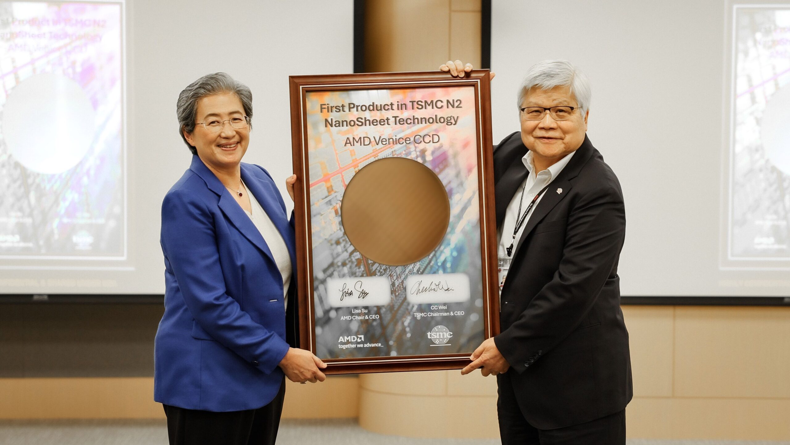
AMD has confirmed that their next-generation Zen 6 EPYC “Venice” CPUs have taped out at TSMC. These CPUs will use TSMC’s 2nm (N2) technology, confirming that AMD is skipping TSMC’s 3nm (N3) node with its Zen 6 CPUs. Today’s Zen 5 EPYC Turin processors use TSMC’s 4nm (N4) technology.
AMD’s “Venice” CPUs will be part of the company’s 6th Generation EPYC CPU platform. They will feature Zen 6 CPU cores and are on track to launch next year.
AMD also confirmed that it has validated its 5th-generation EPYC CPUs at TSMC’s Arizona manufacturing site. This will bring the production of some of AMD’s Zen 5 EPYC CPUs inside the US. This will allow AMD to avoid potential US tariffs on its processors.
✅ Our next-gen EPYC processor, codenamed “Venice,” is the first HPC product in the industry to be taped out and brought up on the TSMC advanced #2nm (N2) process technology.
— AMD (@AMD) April 14, 2025
This news validated recent reports that AMD’s Zen 6 CPUs would use TSMC 2nm technology. These reports also claimed that AMD was aiming for 6+ GHz clock speeds from its Zen 6 Ryzen series processors. Furthermore, these new CPUs reportedly feature more cores per CCD chiplet. With Zen 6, each CPU CCD should feature 12 cores instead of eight.
You can join the discussion on AMD’s validation of “Venice” silicon on TSMC’s 2nm lithography node on the OC3D Forums.