


Nvidia RTX 5090 PCB leaks – Confirms HUGE memory config

Nvidia RTX 5090 PCB confirms the GPU’s huge 32GB frame buffer and more
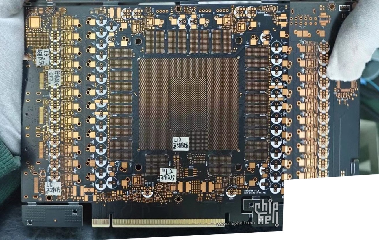
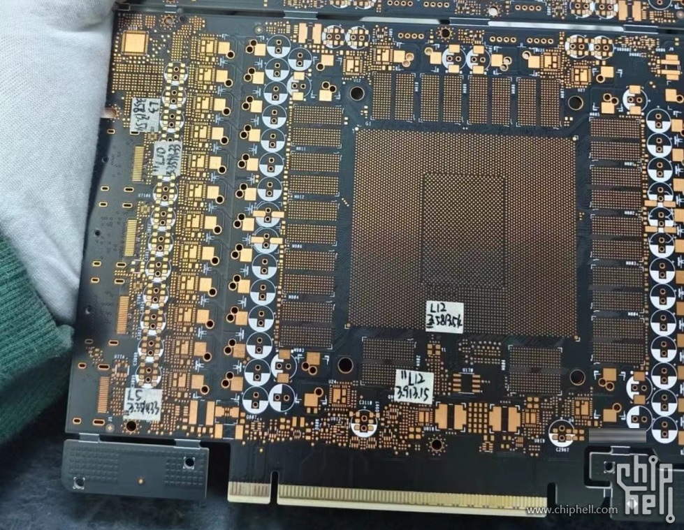
Thanks to 9550pro, we have gotten a look at images of an Nvidia GeForce RTX 5090 PCB. This PCB confirms many of the previously leaked specifications of Nvidia’s next-generation GPU flagship. This includes its use of a large 512-bit memory bus and its huge 32GB GDDR7 frame buffer.
Below, we can see a large GPU package surrounded by sixteen mounting points for GDDR7 memory modules. With standard 2GB modules, Nvidia’s RTX 5090 has 32GB of GDDR7 memory over a 512-bit memory bus. Should Nvidia use 3GB GDDR7 modules, this GPU will have 48GB of GDDR7 memory.
The image above also shows that Nvidia’s new RTX 5090 GPU will use a single 12V-2×6 power connector. This power connector can deliver a maximum of 600 watts of power to a graphics card. That means that we should not expect this GPU to consume over 600 watts of power.
(Nvidia RTX 5090 PCB – via Chiphell Forums)
Assuming that prior 5090 leaks are accurate, Nvidia’s new flagship will have 21,760 CUDA cores. That’s 32.8% more CUDA cores than Nvidia’s RTX 4090. If Nvidia’s new flagship uses 28 Gb/s GDDR7 memory, it will have 77.7% more memory bandwidth than Nvidia’s RTX 4090.
Based on this leak, Nvidia’s next-generation flagship will be a BIG GPU. With a larger GPU package and more connected memory chips, it’s probable that Nvidia’s new flagship will be more expensive than its predecessor. After all, we don’t expect Nvidia to take a margin hit on their new flagship product. Remember, Nvidia’s competitors aren’t releasing products that will compete with their new 5090 GPU. Sadly, that means that Nvidia has no reason to push for lower prices.
You can join the discussion on Nvidia’s leaked RTX 5090 PCB on the OC3D Forums.