RAMBUS launches their HBM3 memory standard to deliver data rates of up to 8.4 Gbps
RAMBUS launches their HBM3 memory standard to deliver data rates of up to 8.4 Gbps
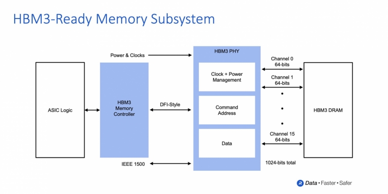
With performance levels of 8.4 Gbps per pin across sixteen 64-bit memory channels, a single HBM3 module can deliver 1.075 TB/s of total bandwidth. In GPU terms, that level of bandwidth is greater than that of an RTX 3090’s memory setup, which delivers 936.2 GB/s of total memory bandwidth using 19.5 Gbps GDDR6X memory. That’s right; a single HBM3 memory chip can deliver more memory performance than Nvidia’s RTX 3090.Â
With their HBM3 standard, RAMBUS has delivered everything that memory makers and chip designers need to create their own HBM3 modules and HBM3-compatible products. HBM3 will be a big deal for graphics card manufacturers, as high levels of memory bandwidth are required to power the next generation of machine learning/artificial intelligence accelerators, FPGAs, and graphics cards.Â
While HBM has been absent from the consumer GPU market for several product generations, it has proven to be a vital part of the enterprise and HPC (High-Performance Computing) markets, which require obscene levels of memory bandwidth to achieve peak performance levels.Â
Â
RAMBUS’ HBM2E standard promised modules with 3.6 Gbps per pin data rates and 461 GB/s per module date rates. HBM3 clearly blows this data rate out of the water, delivering more than a 2x boost in per module memory bandwidth.Â
What follows is RAMBUS’ HBM3 Press Release.Â
 Â
Rambus Advances AI/ML Performance with 8.4 Gbps HBM3-Ready Memory Subsystem
– Provides HBM3-ready memory subsystem solution consisting of fully-integrated PHY and digital controller
– Supports data rates up to 8.4 Gigabits per second (Gbps), enabling terabyte-scale bandwidth accelerators for artificial intelligence/machine learning (AI/ML) and high-performance computing (HPC) applications
– Leverages market-leading HBM2/2E experience and installed-base to speed implementation of customer designs using next-generation HBM3 memory
Rambus Inc., a premier chip and silicon IP provider making data faster and safer, today announced the Rambus HBM3-ready memory interface subsystem consisting of a fully-integrated PHY and digital controller. Supporting breakthrough data rates of up to 8.4 Gbps, the solution can deliver over a terabyte per second of bandwidth, more than double that of high-end HBM2E memory subsystems. With a market-leading position in HBM2/2E memory interface deployments, Rambus is ideally suited to enable customers’ implementations of accelerators using next-generation HBM3 memory.
“The memory bandwidth requirements of AI/ML training are insatiable with leading-edge training models now surpassing billions of parameters,” said Soo Kyoum Kim, associate vice president, Memory Semiconductors at IDC. “The Rambus HBM3-ready memory subsystem raises the bar for performance enabling state-of-the-art AI/ML and HPC applications.”
Rambus achieves HBM3 operation of up to 8.4 Gbps leveraging over 30 years of high-speed signaling expertise, and a strong history of 2.5D memory system architecture design and enablement. In addition to the fully-integrated HBM3-ready memory subsystem, Rambus provides its customers with interposer and package reference designs to speed their products to market.
“With the performance achieved by our HBM3-ready memory subsystem, designers can deliver the bandwidth needed by the most demanding designs,” said Matt Jones, general manager of Interface IP at Rambus. “Our fully-integrated PHY and digital controller solution builds on our broad installed base of HBM2 customer deployments and is backed by a full suite of support services to ensure first-time right implementations for mission-critical AI/ML designs.”
Benefits of the Rambus HBM3-ready Memory Interface Subsystem:
– Supports up to 8.4 Gbps data rate delivering bandwidth of 1.075 Terabytes per second (TB/s)
– Reduces ASIC design complexity and speeds time to market with fully-integrated PHY and digital controller
– Delivers full bandwidth performance across all data traffic scenarios
– Supports HBM3 RAS features
– Includes built-in hardware-level performance activity monitor
– Provides access to Rambus system and SI/PI experts helping ASIC designers to ensure maximum signal and power integrity for devices and systems
– Includes 2.5D package and interposer reference design as part of IP license
– Features LabStation development environment that enables quick system bring-up, characterization and debug
– Enables the highest performance in applications including state-of-the-art AI/ML training and high-performance computing (HPC) systems
You can join the discussion on Rambus’ HBM3 standard on the OC3D Forums.Â


