SK Hynix brings in EUV equipment for its future 1anm DDR5 DRAM modules
SK Hynix brings in EUV equipment for its future 1anm DDR5 DRAM modules
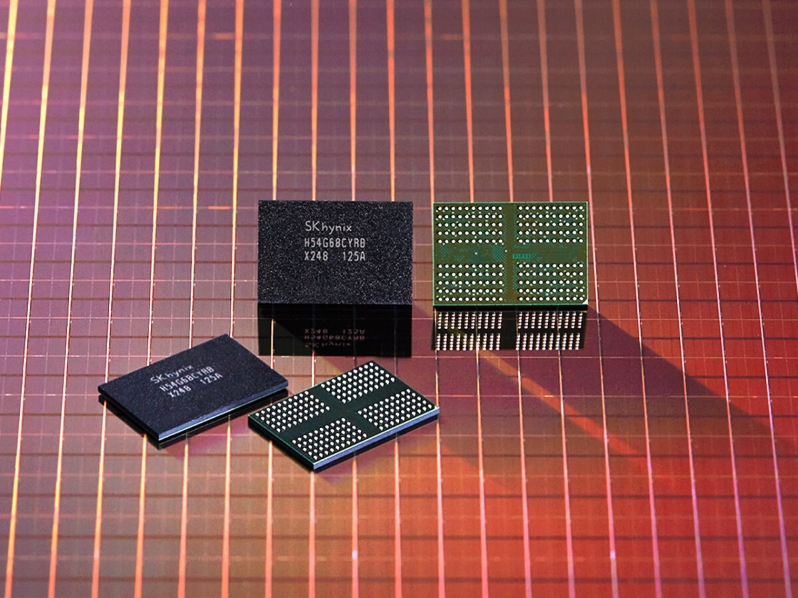
How semiconductor companies utilise their EUV equipment will help to define which companies will have the strongest product offerings over the next decade, and SK Hynix are moving to bring EUV technology to its DRAM product lines. With their new 1a technology, their 4th generation 10 nm DRAM manufacturing technology, SK Hynix had adopted EUV equipment for its cutting-edge DRAM technologies, bringing the technology into mass production.Â
With their 4266 Mbps LPDDR4 DRAM, SK Hynix has reported that their 1anm technology can deliver a 25% increase in wafer productivity and create LPDDR4 DRAM chips that consume 20% less power. These changes allow SK Hynix to create more DRAM chips per silicon wafer and reduce the power usage and ecological impact of the devices using their latest DRAM chips.Â
While much of SK Hynix’s press release focused on their 1anm LPDDR4 DRAM, which is due to be available to customers in the second half of this year, we have found SK Hynix’ discussion of DDR5 DRAM to be of more interest. SK Hynix’s 1anm technology will be applied to their DDR5 memory products in early 2022, which is when DDR5 memory will start to become more widely adopted by the PC industry. Â
 Â Â
 Â
What follow’s is SK Hynix’s Press Release
SK hynix announced that it has started this month mass production of the 8 Gigabit (Gb) LPDDR4 mobile DRAM based on the 1anm, which is the fourth generation of the 10 nm process technology. As the semiconductor industry classifies the 10 nm DRAM products, naming them after the alphabets, the 1a technology is the fourth generation, following the first three generations of the 1x, 1y, and 1z. SK hynix plans to provide the latest mobile DRAM products to smartphone manufacturers from the second half of 2021. This is the first time that SK hynix adopted the EUV equipment for mass production after proving the stability of the cutting edge lithography technology through partial adoption for its 1ynm DRAM production.
As technology migration continues to ultra-micro levels, an increasing number of semiconductor companies are adopting the EUV equipment for the photo process where circuit patterns are drawn on the wafer surfaces. Industry experts believe that a semiconductor company’s leadership in technology will depend on how it can fully take advantage of the EUV equipment. SK hynix plans to use the EUV technology for production of all its 1anm DRAM products going forward as it has proved the stability of the process.
SK hynix expects the new technology to bring an improvement in productivity, and further boost cost competitiveness. The company expects the 1anm technology to lead to a 25% increase in the number of DRAM chips produced from the same size of a wafer, compared with the previous 1znm node. SK hynix anticipates that the 1anm DRAM will also likely help alleviate the supply and demand conditions of the global markets following an increase in DRAM demand globally.
The new product stably runs 4266 Mbps, the fastest transfer rate in a standard LPDDR4 mobile DRAM specification, and has reduced power consumption by 20%. It is a meaningful accomplishment for SK hynix as it aims to reduce carbon dioxide emission as part of its commitment to the environmental, social and governance (ESG) management.
SK hynix will apply its 1anm technology to its DDR5 products, the world’s first next-generation DRAM launched in October 2020, from early next year.
You can join the discussion on SK Hynix’s EUV DRAM plans on the OC3D Forums.Â


