


Intel jumps ahead with next-gen High NA EUV machine install

Intel pushes forward with the world’s first commercial High-NA EUV lithography machine installation
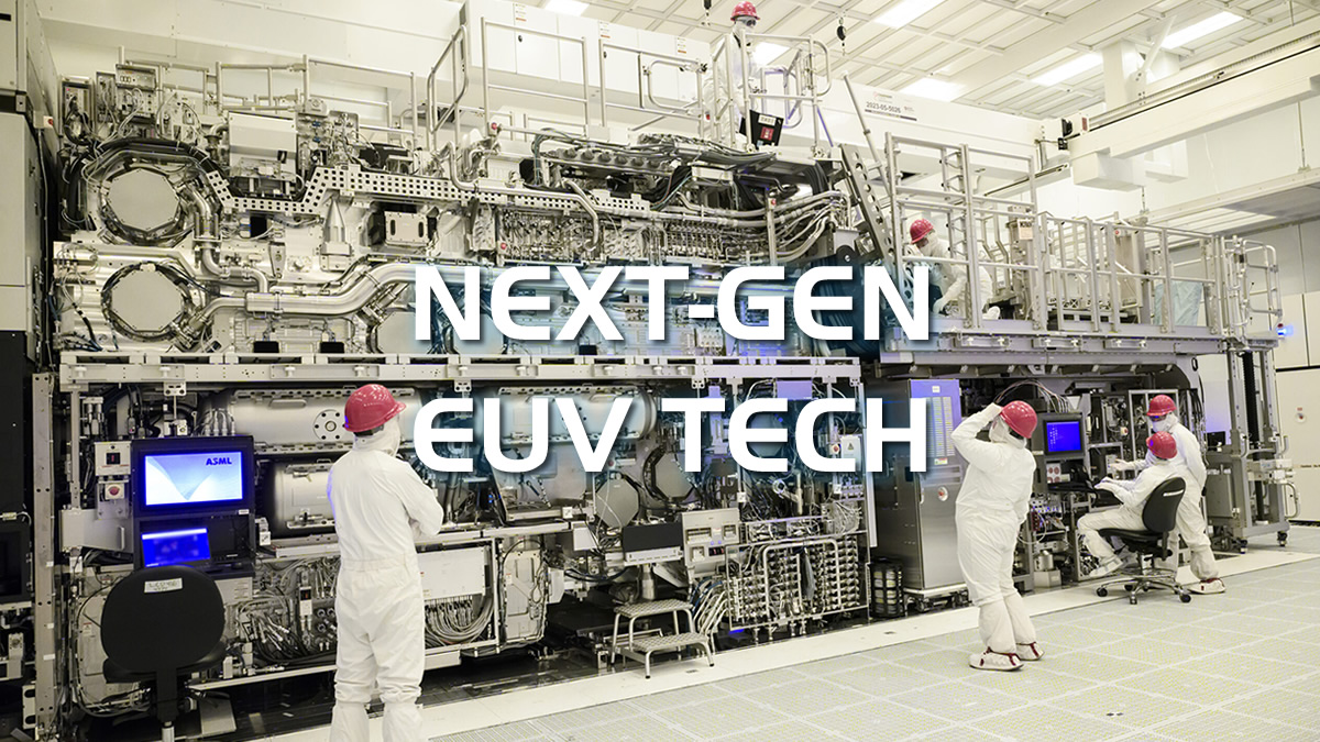
Intel has confirmed that it has installed ASML’s Twinscan EXE:5200B, the industry’s first High-NA lithography tool for commercial chip production. The tool has now passed “acceptance testing”, and will be used to develop Intel’s next-generation lithography nodes. Intel’s 14A node could be its first High-NA EUV node.
Last year, Intel installed ASML’s first-generation EXE:5000 High-NA EUV machine for research purposes. With their new TWINSCAN EXE:5200B, AMSL has retained the same level of detail while increasing productivity with a higher power EUV light source, a new wafer stocker architecture, and tighter alignment controls. In other words, the new tool can work faster, more consistently, and more accurately.
Specifically, today we are excited to share that Intel and ASML have reached the milestone of “acceptance testing” on the TWINSCAN EXE:5200B. This High NA EUV tool maintains the high resolution of the first-generation EXE:5000, while expanding output to 175 wafers per hour and improving overlay (accurate alignment of different lithography layers) to 0.7 nanometers. This builds on Intel’s experience with High NA EUV that began in 2023 with the shipment of the world’s first commercial High NA tool to our research and development fab in Oregon.
– Intel
Intel is moving past standard EUV technology. With High NA EUV tooling, Intel has built a new foundation for its lithography technology. With future nodes, Intel wants to deliver high yields and give customers access to new nodes with more flexible design rules. Using this tech, Intel hopes to compete with TSMC. We expect High-NA EUV to be used with Intel’s upcoming 14A lithography node.
(The tech behind EUV machines is insane)
Why High NA EUV tech matters
Recently, news broke that China had built a working EUV machine prototype, with many heralding the end of America-dominated technology. To say the least, these claims are overblown. For starters, China has a prototype made with spare AMSL parts. They can’t build many vital components themselves. Second, their EUV machine has not yet been used to produce functional chips. Third, Western tech giants are already moving beyond standard EUV technology.
High-NA (High Numerical Aperture) EUV is the next generation of EUV technology. There are two ways to increase the resolution of EUV machines. The first is to use a shorter-wavelength light. The second is to improve the optics, control and tooling of their machines. High-NA EUV technology takes the latter approach.
With new tooling, ASML’s new TWINSCAN EXE:5200B machines take EUV lithography to the next level. This enables higher accuracy and allows users to fabricate smaller transistors. This will usher in a new wave of next-generation lithography nodes.
You can join the discussion on Intel’s installation of ASML’s first TWINSCAN EXE:5200B High NA EUV machine on the OC3D Forums.