


Keeping Moore’s Law Alive – ASML’s latest tech will push the limits of EUV lithography

ASML’s High-NA EUV technology is coming to keep Moore’s Law alive
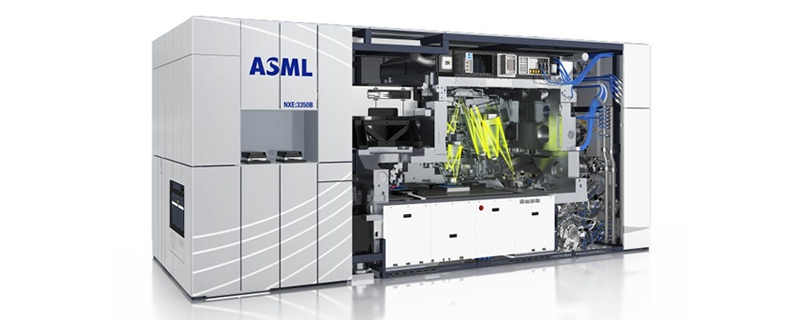
Cutting edge semiconductors require cutting-edge lithography equipment, tools that can be used to build chips with transistors that are unimaginably small and have a level of precision that is crazy high. ASML is one of the companies behind these cutting-edge chipmaking tools, and they are getting ready to deliver next-generation tools that will enable to creation of smaller, more advanced chips.Â
To succeed their Extreme Ultra-Violet (EUV) technology, ASML are working on new high-numerical-aperture EUV (High-NA EUV) lithography tools that will enable the creation of more advanced lithography notes from companies like TSMC, Samsung, Intel, and other chipmaking foundries. All of today’s most advanced chips are currently made using today’s EUV lithography tools, and High-NA EUV tools will help enable the creation of more powerful semiconductors.Â
ASML has confirmed that they plan to have their High-NA EUV lithography tools ready for commercial use in 2025, allowing chipmakers to benefit from these advanced tools in the latter half of this decade. These tools will help keep Moore’s Law alive during the Angstrom era of lithography nodes.
What does High-NA EUV bring to the table?Â
The purpose of ASML’s advanced lithography tools is to allow manufacturers to create chips with smaller and smaller details. The smallest features that ASML’s tools can create is defined by the “critical dimension” of their tools, and there are two primary ways that ASML can decrease the size of these details. The first is to decrease the wavelength of the light that is used to create these lithographic details, and the second is to improve the optics, control and tooling of their machines to increase the accuracy and resolution of their tools.Â
One of the best ways that ASML can improve the resolution of their lithography tools is to increase the numerical aperture of their tools. This is why ASML’s next-generation lithography machines are called high-numerical-aperture EUV (High-NA EUV) machines. With their new tools, ASML wants to push the capabilities of their Extreme Ultra-Violet lithography tools.Â
Once ASML has pushed their EUV technology as far as it can go, ASML will consider changing the wavelength of their lithography tools, moving beyond the “Extreme Ultra-Violet” (EUV) light that they currently use. This will not be a simple process, as it took a long time for the semiconductor industry to advanced EUV technology enough to make it ready for the mass production of semiconductors. Â
To create cutting-edge semiconductors, companies like ASML are working to beat the laws of physics into submission. Frankly, it is astounding that humanity is creating semiconductors with nanometre level precision, and even more astounding that we are aiming for even higher levels of accuracy.
Thanks to ASML’s announcement, we now know that High-NA EUV lithography tools will be ready for production in 2025, and those tools will enable another leap in semiconductor performance, and power efficiency. Better still, ASML believes that they can push their extreme ultraviolet technology in the future.Â
You can join the discussion on ASML’s High-NA EUV chipmaking tools on the OC3D Forums. Â