


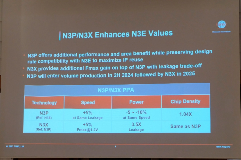
TSMC details the performance uplifts offered by their 3NP and N2 nodes

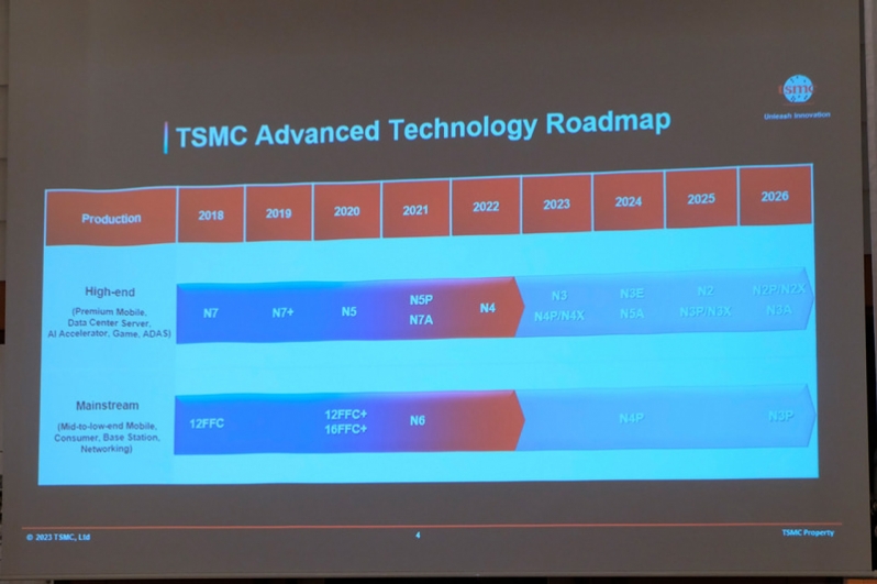
TSMC’s N3E and N3P nodes are on schedule and 2nm should enter mass production by 2025
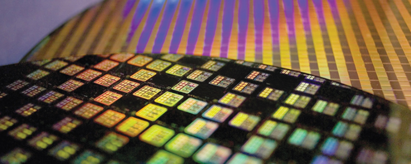
TSMC is currently the world’s leading semiconductor manufacturing company, with their lithography technology being used by companies like AMD, Nvidia, and Apple to create their highest-end computer chips. In recent years, TSMC has significantly increased its R&D investments to help maintain this position, and as part of a media briefing, TSMC’s Kevin Zhang discussed the company’s lithography roadmap.Â
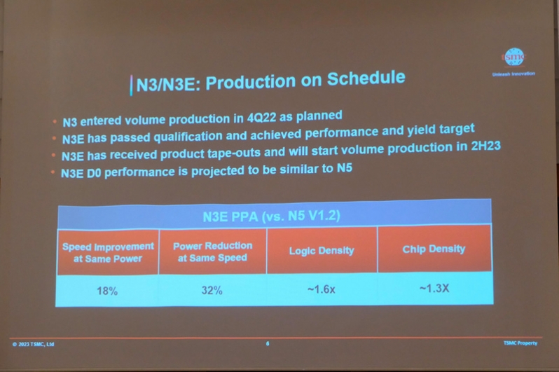
Today, TSMC are creating products using their N3 (3nm) lithography node, though many of TSMC’s customers are utilising the company’s N5 and N4 nodes to create their higher-end chip designs. A improved version of N3, N3E, will be ready to enter mass production later this year, paving the way towards greater N3-class node utilisation by chipmakers. Â
With their N3 lithography node, TSMC expects customers to achieve an 18% performance boost at the same power as an equivalent N5 chip, or to offer customers a 32% decrease in power draw while offering the same performance levels. Logic density for N3E is said to be 1.6x that of N5, and overall chip density is said to be 1.3x greater.Â
Using TSMC’s new N3E lithography node, TSMC expects its customers to be able to create more powerful and more power efficient products. Beyond that, TSMC plans to boost the capabilities of their N3-class lithography nodes further with their enhanced N3P and N3X lithography nodes. Â
Overall, N3P and N3X are very similar to TSMC’s N3 and N3E lithography nodes, which chip density seeing a small increase. These enhanced nodes are designed to increase the potential performance levels that N3-class chips can offer, enabling the creation of powerful products for workstation, desktop, or HPC (High Performance Computing) applications.Â
N3P is set to enter mass production in the second half of 2024, with N3X entering mass production sometime in 2025. Â
In 2025, TSMC’s N2 lithography node is due to enter volume production, moving TSMC away from FinFET transistors and towards nanosheets. When compared to N3E, N2 is expected to offer users 25-30% power reductions while offering users the same speeds, or a 10-15% performance boost at the same power. Chip densities are also expected to increase by 1.15x or more with N2.

With each new lithography node, TSMC aims to allow their customers to squeeze more performance from their future chip designs and reach ever increasing performance heights.Â
You can join the discussion on TSMC’s next-generation process nodes on the OC3D Forums.