


SK Hynix starts mass producing the “world’s first” 128-layer 4D NAND chips

SK Hynix starts mass producing the “world’s first” 128-layer 4D NAND chips
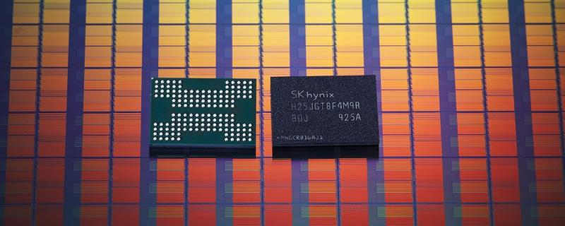
SK Hynix has announced that they have started to mass produce the world’s first 1Tb 128-layer TLC NAND chips using their 4D CTF-based (Charge Trap Flash) NAND flash technology. Why 4D? SK Hynix 4D technology moves a structure known as the periphery under their 3D NAND technology, creating a PUC (Periphery Under Cell) flash chip. The 4th dimension is the structures that have been moved under SK Hynix’ 3D NAND structure. Yes, this isn’t a real 4D structure…
With the company’s new 128-layer 1Tb chips, SK Hynix can provide increased productivity per wafer, offering 40% gains over the company’s existing 96-layer 4D NAND. In addition to this, SK Hynix has claimed that this technology migration costed 60% less than their previous technological shift, delivering surprising levels of investment efficiency.
SK Hynix plans to ship its 4D NAND in the second half of this year, promising data transfer rates of 1,400 Mbps at 1.2V, enabling high-performance levels for mobile devices. SK Hynix also plans to create a 2TB client SSD in-house using this NAND and an SK Hynix-designed controller chip. 16TB and 32TB NVMe SSDs are also planned for the enterprise market.

Moving forward, SK Hynix plans to develop next-generation NAND with 176 layers of NAND cells, with aims to further increase the company’s productivity per wafer and deliver higher storage capacities per chip.
You can join the discussion on SK Hynix starting mass production of the “world’s first” 128-layer 1Tb 3D/4D NAND chips on the OC3D Forums.