Intel Details their Lakefield Processor Design and Foveros 3D Packaging Tech
Intel Details their Lakefield Processor Design and Foveros 3D Packaging Tech
At CES 2019 Intel also revealed Lakefield, the company’s first Foveros 3D processor, but now Intel has released a new video on their YouTube channel which better explains how their technology works, creating a great starting point for consumers who want to know more about the future of Intel’s mobile products. Now, Intel has released a video on their YouTube channel that explains the technology behind Lakefield. Â
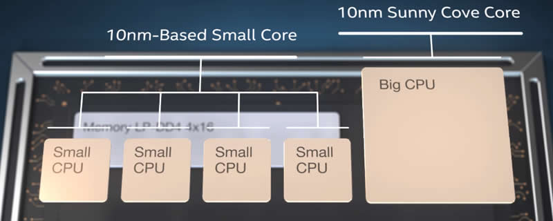
For starters, Intel’s Lakefield CPU is Intel’s first “Hybrid Processor”, offering a single 10nm Sunny Cove processing core alongside four smaller 10nm CPU cores. This combination enables Intel to deliver plenty of multi-threaded performance within a low power envelope while also providing their latest CPU IP for single-threaded scenarios, creating a low-power processor which offers incredible levels of versatility.Â
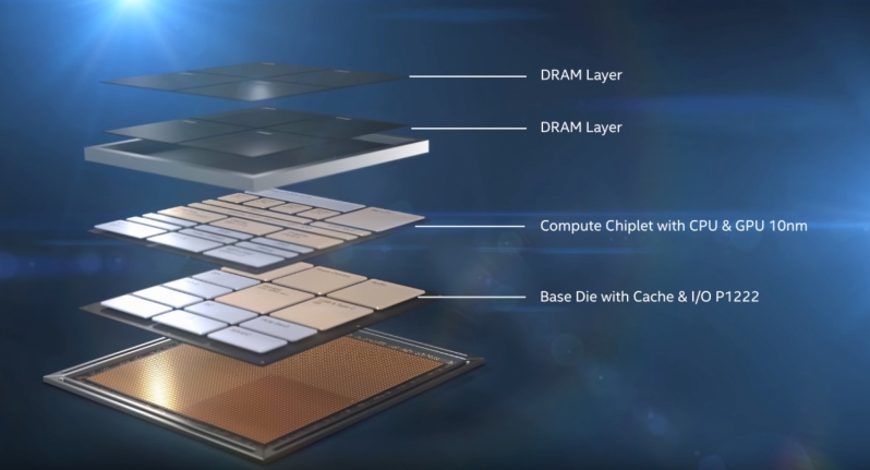
Intel’s Lakefield processor design is said to be 12mm by 12mm in size, which is an amazing feat given the package’s inclusion of I/O on its bottom layer, CPU and graphics IP in the middle and DRAM on the top of the processor. Within this tiny package, Intel has fitted everything that a PC needs, which opens the door to a new range of ultra-mobile PCs.Â
  At CES 2019, Intel previewed a new client platform, code named “Lakefield,†featuring the first iteration of its new innovative Foveros 3D packaging technology. This hybrid CPU architecture enables combining different pieces of IP that might have previously been discrete into a single product with a smaller motherboard footprint, which allows OEMs more flexibility for thin and light form factor design. Lakefield is expected to be in production this year.
While other companies have made pseudo-3D processor before, which are typically referred to as 2.5-D, Intel is the first to build a CPU that operates on several levels, rather than use a silicon interposer to connect several chips on a single level.
Unlike products like AMD’s Vega series of graphics cards, the base layer of Intel’s Foveros package isn’t mostly dead silicon with a variety of interconnects, it is the I/O section of the processor, containing caches, PCIe connection points and other important circuitry. Beyond that, there is also a DRAM later that sits on top of Lakefield’s compute chiplet, delivering insane levels of chip density. Â
At this time it is unknown when Intel’s competitors will be able to offer anything that utilises a fully 3D structure, though AMD has used 2.5-D chips for several generations, starting with their R9 Fury series of graphics cards and multi-chip processor designs since the release of EPYC and Ryzen Theadripper.Â
Intel plans to produce Lakefield silicon this year for use in consumer products, delivering 10nm products in a unique 3D package. With Foveros Intel hopes to revolutionise the mobile PC market with a Hybrid CPU design, Generation 11 graphics, their latest Sunny Cove CPU architecture and their cutting-edge 10nm lithography.Â
More information about Foveros is available here.Â
You can join the discussion on Intel’s Lakefield Processors and 3D Foveros packaging on the OC3D Forums.Â


