


Nvidia’s A100 Tensor Core GPU has a lot of untapped potential

Nvidia’s A100 Tensor Core GPU has a lot of untapped potential
What we’re saying is that Nvidia has left its GA100 GPU core with a lot of unused silicon, so much so that almost 20% of this graphics card’s performance has been locked away. We will explain later why Nvidia may have done this, but it highlights how much potential GA100 still has to offer its potential userbase.
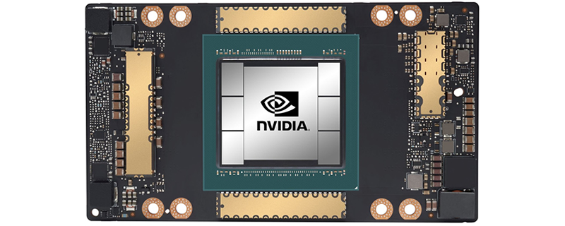
Looking at the block diagram below, we can see that Nvidia’s GA100 core design features a maximum of 128 SMs and six HBM2 memory controllers, offering users a maximum of 48GB of HBM2 memory (with 8GB modules) and 8,192 CUDA cores. That’s a lot more than the 40GB of VRAM and 6,912 CUDA cores that Nvidia’s delivering with its A100 Tensor Core GPU.
Nvidia could release a fully unlocked A100 chip at a later date, or a variant which leaves less of this GPU’s silicon disabled. Given the size of this chip, it is likely that Nvidia has disabled some to GA100’s SMs and memory controllers to help increase silicon yields. That said, disabling over 1,280 CUDA cores is a big cut to make for the sake of yields.
If GA100 was fully unlocked, Nvidia would be able to offer its customer 18.5% more CUDA cores and a 20% increase in memory bandwidth/capacity. Assuming clock speeds remain the same, a fully unlocked GA100 chip could deliver an 18.5-20% performance boost depending on the workload.
At this time it is unknown why Nvidia has locked down so much of its GM100 chips with its A100 Tensor Core GPU. Silicon yields are a likely culprit for the A100’s unused silicon. Perhaps we can expect Nvidia to release a further unlocked A100 Super graphics card next year.

You can join the discussion on Nvidia’s A100 Tensor Core GPU on the OC3D Forum.