


AMD are confirmed to be using 14nm FinFET for their Next generation Polaris GPUs

AMD are confirmed to be using 14nm FinFET for their Next generation Polaris GPUs
Â
AMD have now confirmed that they will be using the 14nm FinFET processing node for their upcoming Polaris GPUs, allowing AMD’s next generation GPUs to be much more power efficient than ever before.Â
Alongside this change in the transistors/ processing node used AMD have worked to build a completely new architecture in order to take advantage of the new FinFET transistors and have “uplifted the frequency of the product” and greatly improved their efficiency, which are both things to see coming from AMD.Â
Â
AMD is proud to introduce our revolutionary 14nm FinFET Polaris GPU architecture. AMD’s Polaris architecture-based 14nm FinFET GPUs a historic leap in performance per watt of Radeon™ GPUs. Polaris architecture-based GPUs are set to deliver smooth frame rates for graphics, gaming, VR and multimedia applications, evolve and compress desktop PC form factors and acoustics, and fuel powerful thin-and-light notebooks.
Â
Â
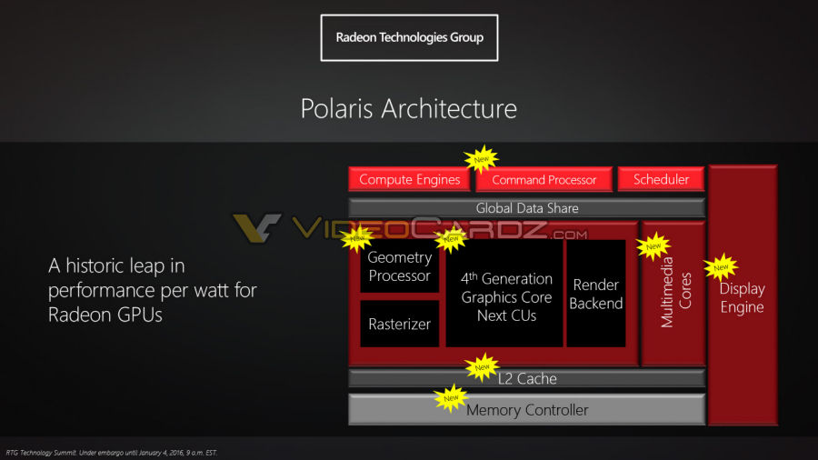
The new Polaris, GCN 4.0 architecture will feature a newly designed command processor, a dedicated multimedia section, a new display engine, geometry processors and a updated memory controller and set of L2 cache, all of which will be instrumental in giving AMD more performance in this upcoming generation of GPUs.
The new command processor will likely help AMD with Asynchronous computing tasks with the new DirectX 12 API, promising that the GPU will never be sitting at idle and the new memory controller will no doubt help AMD make the most out of every bit of memory bandwidth that they can get their hands on with HBM 2.0. Â
AMD has also stated that they have “uplifted the frequency of the product”, meaning that AMD’s upcoming GPUs will be able to run at higher frequencies than before, so perhaps this will mean that AMD will enter an overclocking golden age or simply just have much better clock speeds out of the box. Perhaps 1250MHz or more on the GPU core.Â
Â
Â
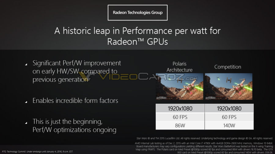
AMD have stated that their new Polaris GPUs have a much greater efficiency than even Nvidia’s Maxwell Architecture, though as always we recommend that you exercise caution when looking at figures that are provided by the maker of one of the products.Â
AMD stated that their new Polaris Architecture GPU system ran at 86 when compared to the Nvidia GTX 950 system which  ran at 140W when under the same settings and framerates, but when considering that the GTX 950 has a TDP of 90W we consider these results from AMD to be questionable at best.Â
AMD’s new Geometry processor design will likely give AMD a boost in tessellation performance when compared to their previous generation GPUs, as this has been a place where AMD has been behind Nvidia for several generations and AMD is no doubt working hard to rectify this.Â
This new GPU will also have the ability to encode and decode h.265 media, which hopefully means that AMD will be gaining a dedicated shadowplay functionality within their drivers, instead of relying on dedicated external applications.Â
Â
Â
None the less these efficiency improvements are very impressive from AMD, as last year they stated that their Next generation products after Fiji would have a 2x increase in efficiency. Only time will tell if AMD has reached their lofty goal of a 2x increase in performance per watt then Polaris GPUs release.Â
This year is going to be a very exciting time for PC gamers, offering us more performance ant lower wattages than ever before for a whole selection of devices. Let’s hope the prices will also be low and competitive, since I really want to see 4K 60FPS this year.Â
Â
You can join the discussion on AMD’s Polaris architecture using 14nm FinFET Transistors on the OC3D Forums.
Â
AMD are confirmed to be using 14nm FinFET for their Next generation Polaris GPUs. https://t.co/KMHVP6unE2 pic.twitter.com/zndcs277Wp
— OC3D (@OC3D) January 4, 2016