


Samsung boosts DRAM density by 50% with sub-10nm breakthrough

Samsung boosts DRAM cell density by 50% with new “4F square cell” tech
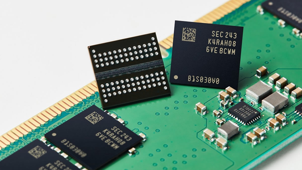
Samsung is reportedly breaking past the 10nm DRAM barrier with its new 10a DRAM technology. Using a new Vertical Channel Transistor (VCT) process, Samsung is reducing the size of its DRAM cells by adding capacitors on top of transistors. Until now, these features were side-by-side, taking up more cell area.
Using its new 10a process, Samsung has created working dies with 4F square cells. These square cells are 2F by 2F, which is much smaller than today’s 6F square cells, which measure 3F by 2F. Thanks to this innovation, Samsung’s DRAM cell area is 50% smaller. This should allow future DRAM chips to be much more memory-dense and cost-effective.
Now that working silicon has been created, Samsung’s next step is to further develop this technology for mass production. This tech should enable 30-50% more DRAM cells to be packed into the same chip areas as before. This should increase DRAM density and wafer productivity. In time, this tech could help lower DRAM prices. It should also help Samsung deliver faster, more power-efficient DRAM.
Samsung Electronics has produced the world’s first single-digit nanometer DRAM working die. It is reported that the company plans to rapidly secure yield by adjusting process conditions based on the working die.
According to industry sources on the 24th, Samsung Electronics reportedly confirmed a working die during the process of inspecting die characteristics after producing wafers using the 10a process last month. This is the result of the first application of the 4F square cell structure and the Vertical Channel Transistor (VCT) process.
– The Elec
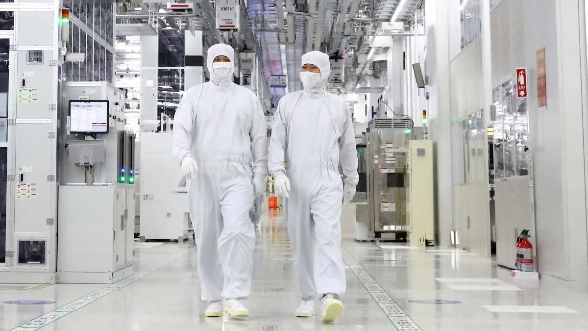
Sadly, Samsung’s new 10a DRAM technology is not a solution to today’s DRAM shortage. It will take time for Samsung to mass-produce DRAM using this technology. After all, Samsung has only recently created working silicon. Regardless, this tech should deliver denser DRAM chips and greater DRAM capacity per silicon wafer. In time, this tech should boost Samsung’s productivity and help lower DRAM prices.
You can join the discussion on Samsung’s 10nm DRAM breakthrough on the OC3D Forums.