Globalfoundries details their 7nm Gen 1-3 process nodes
Globalfoundries details their 7nm Gen 1-3 process nodes
 Â
Â
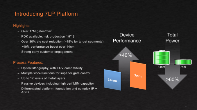
With second generation 7nm, Globalfoundries will add EUV technology to their 7nm platform, though this will not be a full EUV process given the current limitation of EUV manufacturing in high volumes. Â Â
Using a more cautious approach, Globalfoundries will be using EUV technology on key aspects of their 7nm process, with a particular focus on eliminating quadruple patterning from their design wherever possible. This will improve yields for 7nm by reducing complexity and allow manufacturers to bin more chips for lower power or higher performance.
EUV technology will be added to 7nm whenever it is ready, which will likely be in 2018, which means that 1st generation 7nm products will not be designed with EUV in mind. This will mean that we won’t be seeing any EUV products for a while. Â Â Â
Â
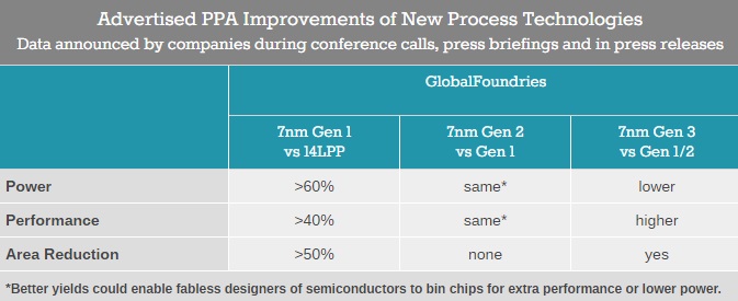
(Tables from Anandtech) Â
Â
With their second-generation EUV 7nm node (3rd generation 7nm), Globalfoundries plans to offer improved LER and resolution to enable higher transistor densities and offer lower power draw and increased performance. Right now performance or density gains are unknown given the experimental nature of this technology.Â
3rd generation 7nm will likely include new design rules to enable the use of greater geometry scaling and higher frequencies, though this is expected to be a fairly easy process of seasoned chip designers. In this node, the majority of layers will still use DUV tech, though increased levels of EUV use are expected. Â
3rd generation EUV nodes are expected around 2020, though this technology will rely on smooth development and Globalfoundries’ ability to work around any issues that they come across.Â
Â
Â
When looking at the roadmap of companies like AMD, we can see that they are planning to work with 7nm in the medium-long term, supporting 7nm with Navi and Zen 2 and planning on using improved nodes line 7nm (likely 7nm gen 2).Â
This should allow AMD to reach performance heights that are beyond what they are capable with 14nm FinFET while allowing them to decrease power draw and achieve higher levels of efficiency.
Â
You can join the discussion on Globalfoundries’ 7nm production plans on the OC3D Forums.Â
Â


