Samsung announces their 11nm LPP and 7nm LPP process nodes

Samsung announces their 11nm LPP and 7nm LPP process nodes
Â
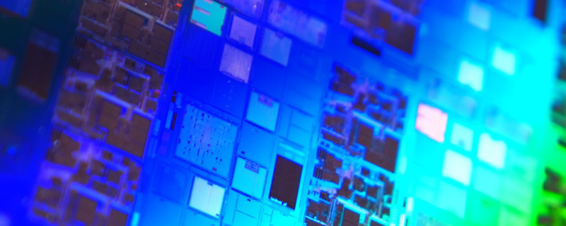
Samsung’s Foundry Division has today revealed two new processing nodes, 11nm LPP (Low Power Plus) FinFET and 7nm LPP FinFET with EUV (Extreme Ultra Violet) technology. Â
Â
11nm LPPÂ is a new process that has been achieved by further scaling their existing 14nm LPP process, with this new node offering up to 10% chip area reductions and 15% higher performance with the same power consumption. This process will be marketed alongside 10nm, with 10nm being intended for premium mobile processors while 11nm is expected to bring more value for value to mid-high-end smart devices.
Â
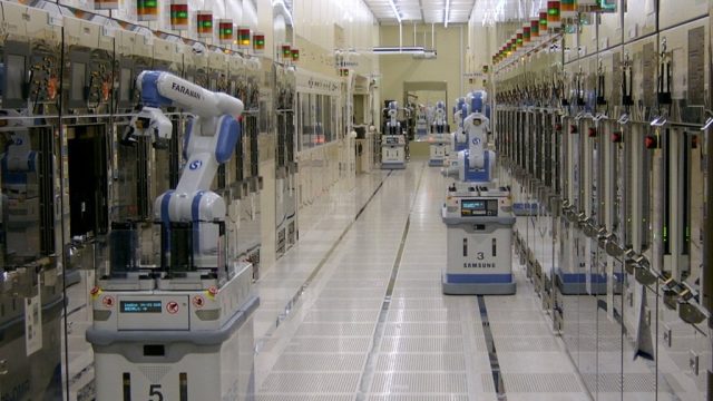
It has been confirmed that Samsung has developed their 7nm LPP EUV process technology on schedule, planning to start initial production in the second half of 2018. Since 2014 Samsung has processed almost 200,000 wafers using EUV lithography, hopefully giving the company enough experience to make a success out of their EUV technology early. Â Â
Â
Â
-
7LPP (7nm Low Power Plus): 7LPP will be the first semiconductor process technology to use an EUV lithography solution. 250W of maximum EUV source power, which is the most important milestone for EUV insertion into high volume production, was developed by the collaborative efforts of Samsung and ASML. EUV lithography deployment will break the barriers of Moore’s law scaling, paving the way for single nanometer semiconductor technology generations.
Â
 Â Â
 Â
More details on these new process nodes are expected to be released later this month at the Samsung Foundry Forum Japan on September 15th.Â
Â
You can join the discussion on Samsung’s new 11nm and 7nm processes on the OC3D Forums.Â
Â


