

Samsung’s new 280-layer QLC NAND aims to make SSDs more affordable and storage dense

Samsung’s latest QLC NAND chips claim to boost data densities far past their rivals
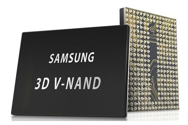
ComputerBase.de has reported that Samsung plans to reveal their new 280-layer QLC NAND chips at the Solid-State Circuits Conference (ISSCC). These NAND chips boast data densities of 28.5 Gb per square millimetre. For context, that is 50% higher than the data density of Micron’s current-generation 232-layer QLC technologies.
With this new NAND, Samsung hopes to power new QLC-powered SSDs that are more data dense and performant than their predecessors. With their new 1 Tb 280-layer QLC NAND chips, Samsung have claimed to offer 3.2 GB/s I/O rates. This is much faster than Samsung’s existing QLC NAND chips, suggesting that the company’s new QLC flash will enable the creation of faster, higher capacity QLC-powered SSDs. Perhaps 16TB M.2 SSDs could be built using this new NAND?
Higher storage speeds and increased data densities will allow Samsung’s new NAND chips to disrupt the SSD market. Higher data densities decrease the cost/GB of NAND flash. In simpler terms, the more Terabytes of NAND that Samsung can get out of a silicon wafer, the better.
We expect to hear a lot more about Samsung’s new NAND chips at the Solid-State Circuits Conference (ISSCC). Will Samsung’s new QLC NAND have the same performance downsides as other QLC chips when hit with sustained writes? Will it rely on SLC caching to maintain high write speeds? Will this NAND be available to SSD manufacturers soon? We will know more soon.
You can join the discussion on Samsung’s 280-layer V9 QLC NAND on the OC3D Forums.