


Samsung speed-boosting 3nm GAAFET transistors aim to boost chip performance


Samsung speed-boosting 3nm GAAFET transistors aim to boost chip performance
What’s the saying? “There’s more than one way to skin a cat?” Well, in the world of transistors, there is more than one way to increase performance. Yes, most of the focus these days is on packing more transistors into tighter spaces, with Intel’s 10nm and TSMC’s 7nm processes garnering a lot of attention, but it must be noted that designs matters.
What do we mean by that? It’s simple, while smaller nodes on more precise and exacting manufacturing standards are positive movements, transistor designs at their core have a significant role to play when it comes to performance. As an industry, the high-end chip market has relied on FinFET transistors for quite some time, and now Samsung believes that they can do better, revealing their 3nm GAAFET (Gate-All-Round FET) manufacturing process.
So what is a GAAFET, a Gate-All-Around transistor? The simple answer is that it takes the idea behind FinFET transistors to the next level, building upon its 3D nature to offer all-around coverage of the transistor’s channel. FinFET, in a basic sense, places a fin within the GATE that has three out of four sides covered, whereas GAAFET transistors have all sides covered. This improved coverage can help lower power losses and increase a transistor’s performance/watt characteristics.
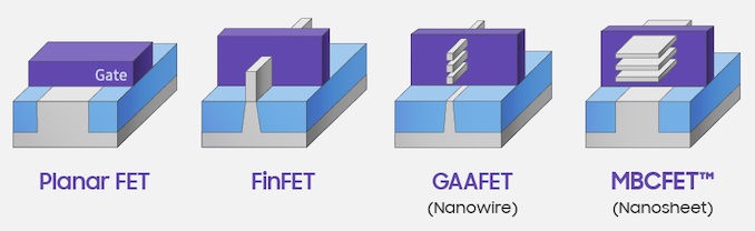
Samsung’s MBCFET transistors are a variant of GAAFET, a name that will be trademarked by the company to denote the manufacturer’s use of Nanosheets instead of Nanowires for their manufacturing. As the image above illustrates, Samsung’s Nanosheet GAAFETs offer a wider design, which is key to Samsung’s performance ambitions.
Smaller Nanosheets can be used for low power designs and wider Nanosheets can be used for high-performance designs, with Samsung allowing manufacturers to utilise up to 4 different Nanosheet widths in single chip designs to offer fine-grained optimisation for each area of a processor.
Samsung has now released version 0.1 of their 3nm GAA MBCFET PDK, allowing companies to get to grips with Samsung’s new design rules and prepare to start using their process when it becomes production ready.

When compared to their 7nm node, Samsung’s 3nm GAA MBCFET mode is said to deliver up to a 50% reduction in power consumption, a 35% increase in transistor performance and a 45% area reduction. While this level of area reduction doesn’t seem that impressive for a so-called 3nm process, Samsung’s 35% performance gain metric is a lot more impressive than what’s currently expected from incoming 5nm nodes. For context, TSMC’s 5nm process is said to offer a 15% performance boost over 7nm.
Samsung’s 3nm GAA MBCFET (3GAE) process will enter risk production in late 2020 and enter volume manufacturing in 2021. A second generation 3nm MBCFET process called 3GAP will enter risk production in 2021 and will likely enter mass production in 2022.
You can join the discussion on Samsung’s speed-boosting 3nm GAAFET transistors on the OC3D Forums.