


TSMC 2nm yields push past 90% as wafer costs reach $30,000

TSMC’s N2 wafers cost 66% more than N3 wafers, and it will only get worse as TSMC moves to N1.4
Wafer pricing is going through the roof at TSMC, with the company’s N2 (2nm) wafers reportedly costing $30,000 each. This is a 66% increase over N3 (3nm), which cost $18,000 per wafer.
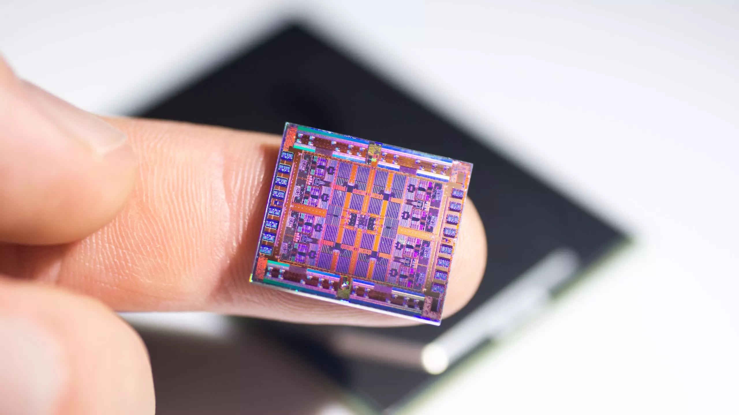
TSMC is making great progress with its N2 lithography node, reporting yields of over 90% on 256Mb SRAM chips. While this yield rate only applies to small SRAM chips (as larger chips always have smaller yields), these numbers are better than what TSMC achieved with its 3N node at the same stage of its development.
The China Times claims that TSMC’s wafer pricing will worsen as the company enters the Angstron era with N1.4 (1.4 nm). Wafer pricing is reportedly set to increase by 50% to $45,000 USD. This puts upward pressure on the cost of high-end electronics, as silicon costs are continuing to grow.
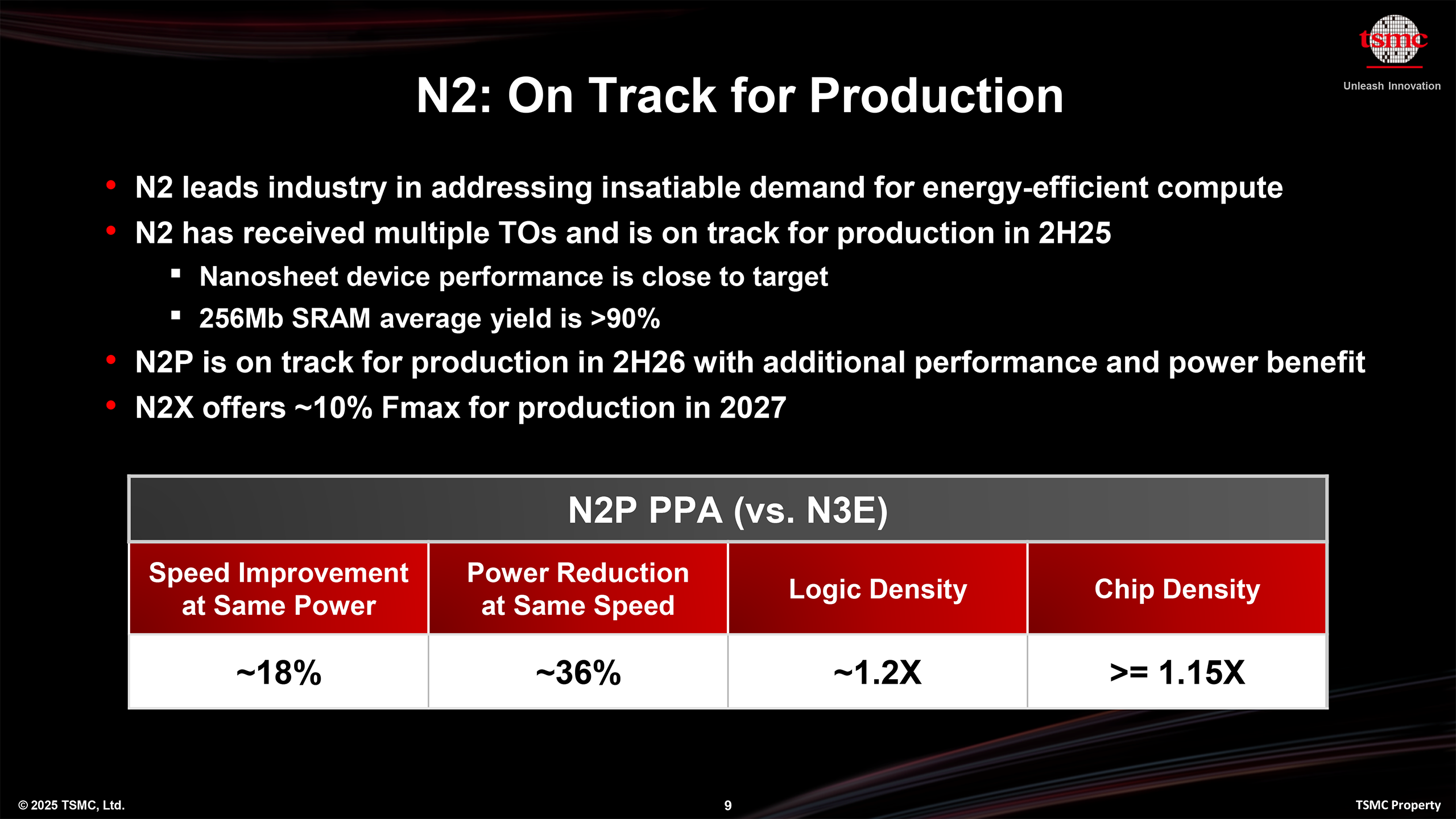
(TSMC reports greater than 90% yields on N2 256Mb SRAM chips)
AMD has confirmed that it will be using TSMC’s N2 (2nm) technology to create its next-generation Zen 6 “Venice” CPUs. This means that AMD is skipping TSMC’s N3 node and moving directly to N2. Clearly, AMD wants the benefits of TSMC N2 (2nm) to ensure that its next-generation Zen 6 CPUs outperform their competition. Clearly, AMD is concerned that Intel may have a strong rival to Zen 6.
You can join the discussion on TSMC’s N2 yields on the OC3D Forums.