


Samsung Mass Producing 4GB HBM2 memory stacks


Samsung Mass Producing 4GB HBM2 memory stacks
Samsung has just announced that they have begun mass production of 4GB DRAM chips using the High Bandwidth memory gen. 2 (HBM2) interface. These new chips are designed for use in high performance compute applications, advanced graphics hardware and enterprise grade systems.
Samsung’s new HBM2 memory offers an higher level of performance when compared to GDDR5, with up to 7 times faster speeds, faster responsiveness and lower power consumption.
This memory will be built on Samsung’s 20nm process technology, giving a great balance between power efficiency, reliability and affordability, while keeping the memory chip small and easy to use.
By mass producing next-generation HBM2 DRAM, we can contribute much more to the rapid adoption of next-generation HPC systems by global IT companies,” said Sewon Chun, senior vice president, Memory Marketing, Samsung Electronics. “Also, in using our 3D memory technology here, we can more proactively cope with the multifaceted needs of global IT, while at the same time strengthening the foundation for future growth of the DRAM market.
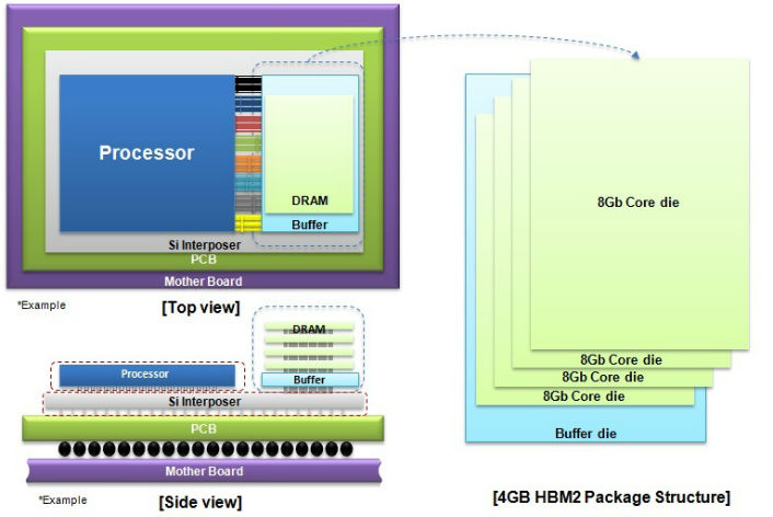
This 4GB module is made by stacking 4 8Gb DRAM dies together vertically, offering 256GBps of bandwidth, double that of HBM1 and more than 7x that of GDDR5.
HBM memory technology is also highly efficient, doubling the bandwidth per watt of GDDR5 and embeds ECC (error correcting code) for enhanced reliability.
With current HBM GPUS like the AMD R9 Fury X using 4x HBM chips, it is expected that next generation HBM based GPUS will have up to 16GB of HBM2 memory.
You can join the discussion on Samsung mass producing their new 4GB HBM2 memory chips on the OC3D Forums.
Samsung Mass Producing 4GB HBM2 memory, with 8GB HBM2 memory coming later this year. https://t.co/3qlUDseVu6 pic.twitter.com/5slFqKtsQ0
— OC3D (@OC3D) January 19, 2016