TSMC accelerates its A14 node (1.4nm) production plan

TSMC is pushing A14 node development forward to put pressure on Intel
UDN has confirmed that TSMC has started constructing its planned A14 (1.4 nm) fab ahead of schedule, targeting risk production for the new node in 2027 and high-volume production in 2028. This new site, known as Fab 25, is situated in the Central Taiwan Science Park, near Taichung, and is expected to feature four production buildings.
So far, TSMC has not commented on why construction has started early. However, there is speculation from industry analysts that TSMC is doing this to “ensure market exclusivity.” By accelerating their timetable, TSMC wants to put more pressure on Intel and deny them customers from their 14A (1.4nm) node. Intel may abandon future lithography nodes if it fails to attract customers with 14A. That alone gives TSMC plenty of incentives to accelerate its development timetable. If TSMC can persuade Intel to exit its foundry business, it will have eliminated one of its only viable competitors.
TSMC A14 Performance
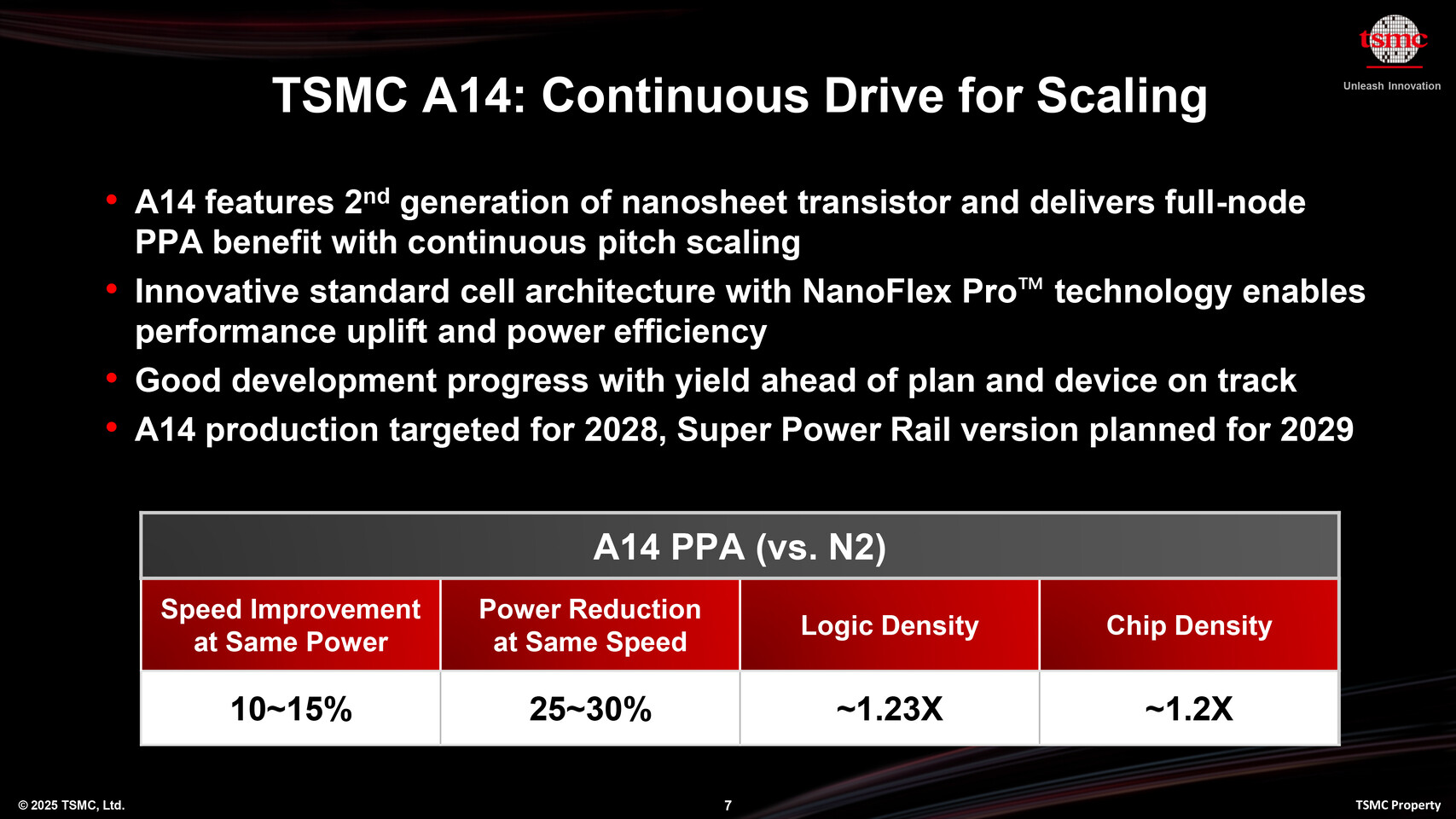
TSMC’s A14 node is expected to deliver a 23% increase in logic density and a 20% increase in overall chip density when compared with their N2 (2nm) node. Performance-wise, TSMC expects 10-15% more performance than N2 at the same power. Alternatively, this node should be able to deliver the same performance as N2, but with 25-30% less power.
With its 1.4A node, TSMC plans to continue to make denser, more performant silicon. If everything goes as planned, this will keep TSMC ahead of its competitors. This will ensure its continued dominance of the silicon foundry market. If TSMC is hit with delays, it could provide an opportunity for its competitors to gain ground.
You can join the discussion on TSMC accelerating its A14 node development on the OC3D Forums.