Nvidia to power its next-gen “Feynman”, GPUs with TSMC A16

Nvidia reportedly plans to use TSMC A16 for its next-generation “Feynman” GPUs
According to a report from the Commercial Times Taiwan, Nvidia now plans to utilise the next-generation A16 node from TSMC to create its planned “Feynman” graphics cards. A16 will be TSMC’s first lithography node to NanoFlex transistors with backside power delivery. This node is due to enter production during the second half of 2026. Nvidia names its GPU after famous scientists, with Feynman being named after the theoretical physicist Richard Feynman.
Nvidia “Feynman” is expected to be the architecture that succeeds Nvidia’s Rubin and Rubin Ultra graphics cards. Today’s Nvidia Blackwell GPUs use TSMC’s N4 (4nm) lithography node. Next year’s Rubin GPUs are due to use TSMC’s N3 (3nm) node. With “Feynman”, Nvidia reportedly plans to skip TSMC’s 2nm node and move straight to A16 (1.6nm).
It has been claimed that Nvidia plans to make this larger lithography node shift due to increased competition. By utilising A16, Nvidia aims to maintain its performance leadership.
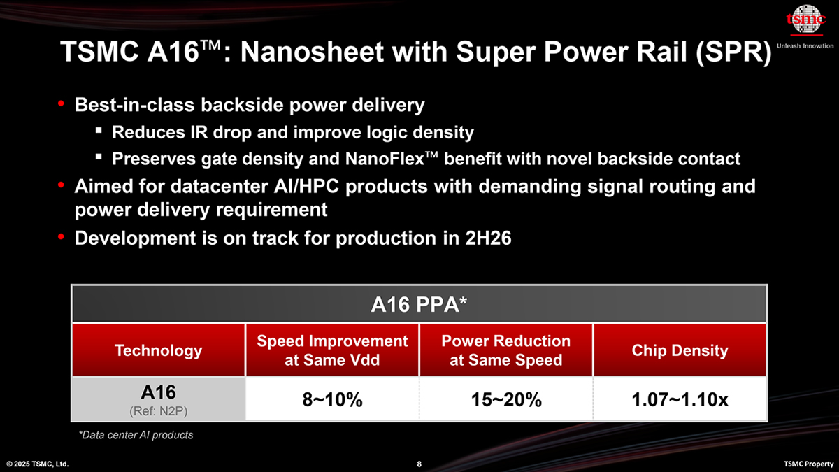
Below, we can see TSMC’s performance characteristics for its A16 node. TSMC expects a 7-10% increase in chip density, an 8-10% performance improvement at the same Vdd, or a power reduction of up to 15-20% while maintaining the same speeds as N2 (2nm).
Currently, it is unclear whether Nvidia’s Feynman GPU architecture will be available to all segments of the GPU market. Will Nvidia’s Feynman be an AI/datacenter-only architecture (like Rubin), or will Feynman see a wider release with GeForce RTX products? Will Nvidia Feynman be Blackwell’s successor?
You can join the discussion on Nvidia’s planned A16 “Feynman” GPUs on the OC3D Forums.