


Additional information on Nvidia’s Volta Tesla V100 GPU

Additional information on Nvidia’s Volta Tesla V100 GPU
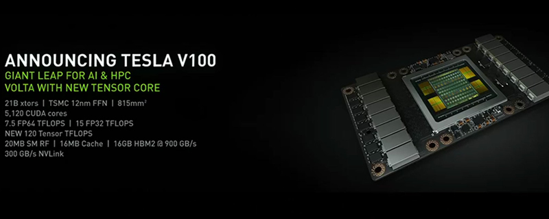
This new GPU will come with a total of 7.5TFLOPs of FP64 compute power and 15TFLOPs of FP32 compute power, which is simply huge for any GPU. This performance is not achieved by increased clock speeds like in Pascal, but by using additional CUDA processors, with the GPU containing a total of 5,120 CUDA cores.
Below is a table comparing Nvidia’s Tesla V100 GPU to last year’s Tesla P100, as well as some recent gaming GPUs from the company. Please note that the gaming oriented GPUs listed have a smaller die size due to their decreased silicon complexity/lack of FP64 compute cores etc.
| Tesla V100 | Tesla P100 | GTX Titan Xp | GTX 1080 Ti | GTX 1080 | GTX 980 Ti | |
| GPU Architecture | Volta | Pascal | Pascal | Pascal | Pascal | Maxwell |
| Process node | 12nm | 16nm | 16nm | 16nm | 16nm | 28nm |
| Die Size (mm^2) | 815mm^2 | 610mm^2 | 471mm^2 | 471mm^2 | 314mm^2 | 601mm^2 |
| FP32 TFLOPs | 15 | 10.6 | 12 | 10.6 | 8.2 | 5.63 |
| Transistor Count | 21.1B | 15.3B | 12B | 12B | 7.2B | 5.2B |
| CUDA Core Count | 5120 | 3584 | 3840 | 3584 | 2560 | 2816 |
| ROPs | 128 (?) | 96 | 96 | 88 | 64 | 96 |
| VRAM Type | HBM2 | HBM2 | GDDR5X | GDDR5X | GDDR5X | GDDR5 |
| Memory Clock | 874MHz | 700MHz | 11408MHz | 11008MHz | 10008MHz | 7000Mhz |
| VRAM Cappacity | 16GB | 16GB | 12GB | 11GB | 8GB | 6GB |
| Memory Bus Size | 4096-bit | 4096-bit | 384-bit | 352-bit | 256-bit | 384-bit |
| Memory Bandwidth | 900GB/s | 720GB/s | 547.7GB/s | 484 GB/s | 320 GB/s | 336GB/s |
| Base clock speed | – | 1328MHz | 1480MHz | 1480MHz | 1607MHz | 1000MHz |
| Boost clock speed | 1455MHz | 1480MHz | 1582MHz | 1582MHz | 1733MHz | 1089MHz |
| TDP | 300W | 300W | 250W | 250W | 180W | 250W |
| Power Connection | – | – | 1x 8-pin 1x 6-pin |
1x 8-pin 1x 6-pin |
1x 8-pin | 1x 8-pin 1x 6-pin |
| PCI Express | NVLink 2.0 | NVLink 1.0 | PCIe 3.0 | PCIe 3.0 | PCIe 3.0 | PCIe 3.0 |

When looking at these specifications we can see that the Tesla V100 comes with a similar design to Nvidia’s Pascal Tesla P100, with the same number of CUDA cores per SM but with a 42% increase in total core count. This results in a huge increase die size, which could result in yield issues for Nvidia.
In manufacturing silicon dies, size is a huge factor. In every silicon wafer there will be defects and when manufacturers make larger chips these defects will harm an ever larger proportion of the chips produced, harming production yield in the process.
Imagine that in a silicon wafer that there are 10 major defects and that when making a small chip that you create 180 dies per wafer, this will result in 10 faulty chips and a failure rate of 5%. Then imagine that you are creating a larger chip and you only get 60 dies per wafer, resulting in the same 10 faulty chips and a failure rate of 16%. These numbers are just for illustration purposes and are not to be taken as actual yield rates at a foundry, but it does illustrate the reason why larger dies are more prone to having faults and therefore suffer from lower yields than silicon with smaller die sizes.

When it comes to die sizes there are also other factors to consider, like the fact that silicon wafers are circular. You can only fit a certain number of square sides within a circle and larger dies will result in additional wasted space at the edges of a silicon wafer. This again reduces the number of dies per wafer and will increase the price of each chip in a wafer.
One interesting thing to note is that the Tesla V100 comes with clock speeds that are 25MHz lower than Nvidia’s Pascal based P100 and over 100MHz lower than the GTX 1080 Ti, which could mean that Volta will not come with a large increase in clock speeds over Pascal.
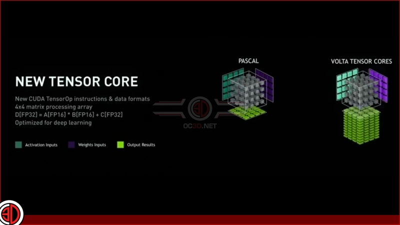
What Nvidia has added in their Volta architecture is a “new Tensor core”, which are designed to benefit Volta when doing mass processing for deep learning. At this time it is unknown how much these new cores will benefit Volta outside of Deep learning, or if they will even be present in Volta’s gaming/consumer Geforce GPUs.
Nvidia claims that their Volta V100 is the largest GPU that can currently be produced using modern process technology, with this new chip easily dwarfing the companies older GPU designs despite using TSMC’s new 12nm process.

Nvidia has been clear that Volta is not just Pascal with Tensor cores, calling Volta their largest GPU redesign since Firmi, though the company has confirmed that their Volta server GPUs will not be releasing until Q3 of 2017.
It is unlikely that we will be seeing consumer Volta anytime before this, especially with the recent releases of the GTX 1080 Ti and Titan Xp.
Even if Nvidia were to try and release a consumer version of Volta within that timeframe it would certainly not be GPUs to the scale shown here, as only with the release of the GTX 1080 Ti have consumers been able to purchase GPUs that have similar core counts to the Pascal P100. Beyond this, it is also unknown if Nvidia plans on releasing consumer versions of Volta with HBM2 or a different memory standard like GDDR6, the latter of which is due to release in early 2018.
You can join the discussion on Nvidia’s Volta architecture and the Tesla V100 on the OC3D Forums.