


AMD’s CTO discusses their move to 7nm

AMD’s CTO discusses their move to 7nm
AMD’s CTO (Chief Technology Officer), Mark Papermaster, has been discussing the company’s move to GlobalFoundries’ 7nm manufacturing process, calling the change the “toughest lift I’ve seen in a number of generations,”.
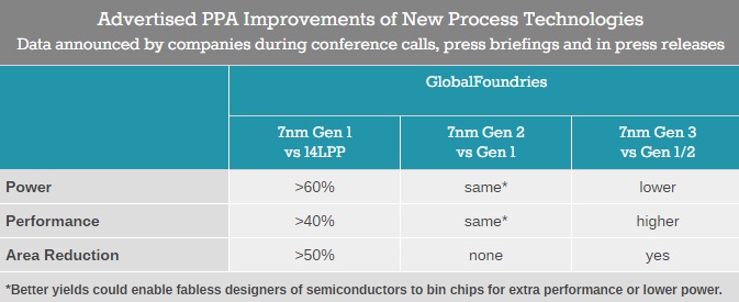
7nm is expected to be the next “long node” which will span several product generations, with Globalfoundries planning three generations of 7nm process nodes, each of which will deliver better yields and increased use of EUV technology, which will reduce the need for quadruple patterning and allow designs to be manufactured at lower costs.
With 7nm Papermaster states that AMD “had to literally double our efforts across foundry and design teams”, with the node requiring new “CAD tools and [changes in] the way you architect the device [and] how you connect transistors—the implementation and tools change [as well as] the IT support you need to get through it”.
Papermaster also says that it was vital for AMD to deepen their partnership with foundries and the EDA community, given the complexity of AMD’s designs and their reliance of quad-patterning on 7nm. This makes it critical for both AMD’s and Globalfoundries’ design teams are in full/perfect communication.
AMD says that they are expecting to adopt EUV technology in 2019, with plans to reduce the need for quad-patterning and greatly reduce the total number of required masks, lowering the costs and shortening the design times of AMD’s future products. Mark Papermaster urges the foundry industry to adopt EUV technology “as fast as they can”.


(AMD’s Zen 2 CPUs and Navi GPUs will be based on 7nm)
Papermaster also calls for the EDA (electronic design automation) community to adapt their software infrastructure to take advantage of more CPU cores and parallelism, as the additional processing required for 7nm designs will make the optimisation of this software vital moving forward.
It looks like AMD requires better hardware utilisation by software to in turn allow them to create more powerful hardware.
my call to action for the EDA community…is to redouble their efforts to take advantage of more CPU cores and parallelism…As the processing required for 7nm escalates…their algorithm optimization needs to take advantage of the very technology they are helping us manufacture,
(7nm offers a lot of advantages over 14nm)
When looking at the roadmap of companies like AMD, we can see that they are planning to work with 7nm in the medium-long term, supporting 7nm with Navi and Zen 2 and planning on using improved nodes line 7nm (likely 7nm gen 2) with their future CPU and graphics products.
This should allow AMD to reach performance heights that are beyond what they are capable with 14nm FinFET while allowing them to decrease power draw and achieve higher levels of efficiency.
You can join the discussion on AMD’s 7nm plans on the OC3D Forums.