


NVIDIA GTX 280 Performance Revealed – MSI N280GTX

Introduction
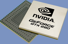 Over the past couple of months, pictures and sketchy information about NVIDIA’s latest flagship GPU have been circulating the internet. While NVIDIA have done their best to keep things quiet, many of us have been holding off on a much needed graphics card purchase to find out exactly what NVIDIA have had up their sleeves. Well, after being fed a flurry of re-hashed technology from both NVIDIA and ATI in the form of their Dual-GPU 3870×2 and 9800GX2 graphics cards, the wait is finally over – and today Overclock3D have managed to get their hands on NVIDIA’s new-gen flagship GPU – the GTX 280.
So, why the change in naming convention I hear you ask? Well after attending NVIDIA’s recent press event, the reason given is that they wanted to mark the fact that these really are a new generation of GPU’s. Calling the GPU a 9900GTX simply didn’t do justice for the number of changes they’ve made, and 10800GTX…is just plain silly. Obviously, NVIDIA will also be releasing lower-end cards based on this architecture later in the year (GTX 230 maybe??) and the current naming convention would not have allowed for this.
 Starting with the basics, NVIDIA have designed the GTX 200 series to be much more than a standard graphics processor. Coining the two phrases “Beyond 3D” and “3D Beyond” as part of the driving force behind the architectural design of the GTX 200, NVIDIA have been demonstrating just how the unbeatable multi-threaded performance of the GPU can be put to good use in applications such as video transcoding or medical research such as [email protected] via CUDA. As many of us will already know, physics processing via the PhysX API is also being transferred over to CUDA and this, combined with the fact that the GTX 200 series is fully Tri-SLI ready, should lead to some very interesting times ahead – in both gaming and general computing.
In terms of actual architectural differences, the GTX 200 series is the first to implement NVIDIA’s second generation unified shader. According to NVIDIA, this offers significantly enhanced features and can deliver on average 1.5x better performance than that of the GeForce 8/9 series. The SPA architecture of the GTX 280 also enters the second-generation, with an increase in the SM’s per TPC from two to three, and an overall increase in TPC’s per chip from 8 to 10. This results in a whopping increase in processor cores to 240 from the original 128 of the G80 and G92. Manufactured using a 65nm fabrication process, the GTX 200 also includes 1.4 billion transistors (more than double that of the 8800GTX).
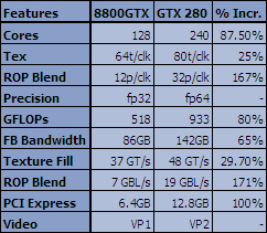 Special attention has also been made to power efficiency with the GTX 200 GPU’s, featuring four different power modes rather than the standard 2D/3D modes found on most other cards. Once again referring to information from NVIDIA, these modes will be: 2D mode with a power consumption of 25w, DVD playback mode with a consumption of 35w, 3D performance mode with a worst-case (TDP) consumption of 236w and support for NVIDIA’s HybridPower mode, which effectively powers down the GPU and switches to an on-motherboard solution.
NVIDIA have also kitted the GTX 280 and 260 with 1GB and 896 MB frame buffers respectively. Ignoring the dual-GPU cards such as the 9800GX2 for one minute, this is an almost double increase in frame buffer from the previous generation cards and should help performance when gaming at high resolutions with anti-aliasing. Memory addressing has also received a bump in spec, with a 512-bit memory interface (up from 384-bit in previous gen) and a modified texture to frame buffer (TEX:FB) ratio to ensure that texture units are not starved for data.
So now that we’ve got all of the formalities out of the way, let’s take a close-up look at MSI’s GTX 280 and find out how all of this new tech translates into FPS figures for our avid gamers…